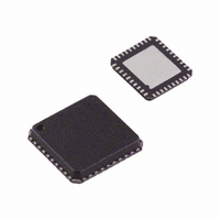
ADUC7020BCPZ62I-RL Analog Devices Inc, ADUC7020BCPZ62I-RL Datasheet - Page 43

ADUC7020BCPZ62I-RL
Manufacturer Part Number
ADUC7020BCPZ62I-RL
Description
IC,MICROCONTROLLER,16-BIT,ARM7 CPU,CMOS,LLCC,40PIN,PLASTIC
Manufacturer
Analog Devices Inc
Series
MicroConverter® ADuC7xxxr
Datasheet
1.USB-I2CLIN-CONV-Z.pdf
(96 pages)
Specifications of ADUC7020BCPZ62I-RL
Core Processor
ARM7
Core Size
16/32-Bit
Speed
44MHz
Connectivity
EBI/EMI, I²C, SPI, UART/USART
Peripherals
PLA, PWM, PSM, Temp Sensor, WDT
Number Of I /o
14
Program Memory Size
62KB (62K x 8)
Program Memory Type
FLASH
Ram Size
8K x 8
Voltage - Supply (vcc/vdd)
2.7 V ~ 3.6 V
Data Converters
A/D 5x12b; D/A 4x12b
Oscillator Type
Internal
Operating Temperature
-40°C ~ 125°C
Package / Case
40-LFCSP
Lead Free Status / RoHS Status
Lead free / RoHS Compliant
For Use With
EVAL-ADUC7020QSZ - KIT DEV ADUC7020 QUICK STARTEVAL-ADUC7020MKZ - KIT MINI DEV FOR ADUC7026/7027
Eeprom Size
-
Lead Free Status / RoHS Status
Lead free / RoHS Compliant
Available stocks
Company
Part Number
Manufacturer
Quantity
Price
Part Number:
ADUC7020BCPZ62I-RL
Manufacturer:
ADI/亚德诺
Quantity:
20 000
Table 18. ADCCON MMR Bit Designations
Bit
15:13
12:10
9:8
7
6
5
4:3
2:0
Value
000
001
010
011
100
101
00
01
10
11
00
01
10
11
000
001
010
011
100
101
Other
Description
Reserved.
ADC clock speed.
fADC/1. This divider is provided to obtain
1 MSPS ADC with an external clock <41.78 MHz.
fADC/2 (default value).
fADC/4.
fADC/8.
fADC/16.
fADC/32.
ADC acquisition time.
Two clocks.
Four clocks.
Eight clocks (default value).
16 clocks.
Enable start conversion.
Set by the user to start any type of conversion
command. Cleared by the user to disable a
start conversion (clearing this bit does not
stop the ADC when continuously converting).
Enable ADC
Set by the user to enable the ADC
Cleared by the user to disable the ADC
ADC power control.
Set by the user to place the ADC in normal
mode (the ADC must be powered up for at least
5 μs before it converts correctly). Cleared by the
user to place the ADC in power-down mode.
Conversion mode.
Single-ended mode.
Differential mode.
Pseudo differential mode.
Reserved.
Conversion type.
Enable CONV
Enable Timer1 as a conversion input.
Enable Timer0 as a conversion input.
Single software conversion. Sets to 000 after
conversion (note that Bit 7 of ADCCON MMR
should be cleared after starting a single
software conversion to avoid further
conversions triggered by the CONV
Continuous software conversion.
PLA conversion.
Reserved.
BUSY
START
.
pin as a conversion input.
BUSY
START
BUSY
pin.
pin).
pin.
Rev. C | Page 43 of 96
Table 19. ADCCP Register
Name
ADCCP
ADCCP is an ADC positive channel selection register. This
MMR is described in Table 20.
Table 20. ADCCP
Bit
7:5
4:0
1
Table 21. ADCCN Register
Name
ADCCN
ADCCN is an ADC negative channel selection register. This
MMR is described in Table 22.
ADuC7019/20/21/22/24/25/26/27/28/29
ADC and DAC channel availability depends on the part model. See Ordering
Guide for details.
Value
00000
00001
00010
00011
00100
00101
00110
00111
01000
01001
01010
01011
01100
01101
01110
01111
10000
10001
10010
10011
Others
Address
0xFFFF0504
Address
0xFFFF0508
1
Description
Reserved.
Positive channel selection bits.
ADC0.
ADC1.
ADC2.
ADC3.
ADC4.
ADC5.
ADC6.
ADC7.
ADC8.
ADC9.
ADC10.
ADC11.
DAC0/ADC12.
DAC1/ADC13.
DAC2/ADC14.
DAC3/ADC15.
Temperature sensor.
AGND (self-diagnostic feature).
Internal reference (self-diagnostic feature).
AV
Reserved.
MMR Bit Designation
DD
/2.
Default Value
0x00
Default Value
0x01
Access
R/W
Access
R/W


