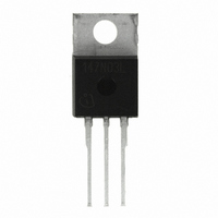
IPP147N03L G Infineon Technologies, IPP147N03L G Datasheet - Page 3

IPP147N03L G
Manufacturer Part Number
IPP147N03L G
Description
MOSFET N-CH 30V 20A TO-220-3
Manufacturer
Infineon Technologies
Series
OptiMOS™r
Datasheet
1.IPP147N03L_G.pdf
(10 pages)
Specifications of IPP147N03L G
Fet Type
MOSFET N-Channel, Metal Oxide
Fet Feature
Logic Level Gate
Rds On (max) @ Id, Vgs
14.7 mOhm @ 20A, 10V
Drain To Source Voltage (vdss)
30V
Current - Continuous Drain (id) @ 25° C
20A
Vgs(th) (max) @ Id
2.2V @ 250µA
Gate Charge (qg) @ Vgs
10nC @ 10V
Input Capacitance (ciss) @ Vds
1000pF @ 15V
Power - Max
31W
Mounting Type
Through Hole
Package / Case
TO-220-3 (Straight Leads)
Transistor Polarity
N Channel
Drain Source Voltage Vds
30V
On Resistance Rds(on)
12.3mohm
Rds(on) Test Voltage Vgs
10V
Voltage Vgs Max
20V
Operating Temperature Range
-55°C To +175°C
Transistor Case Style
TO-220
Rohs Compliant
Yes
Configuration
Single
Resistance Drain-source Rds (on)
0.0147 Ohms
Drain-source Breakdown Voltage
30 V
Gate-source Breakdown Voltage
+/- 20 V
Continuous Drain Current
20 A
Power Dissipation
31 W
Maximum Operating Temperature
+ 175 C
Mounting Style
Through Hole
Minimum Operating Temperature
- 55 C
Lead Free Status / RoHS Status
Lead free / RoHS Compliant
Lead Free Status / RoHS Status
Lead free / RoHS Compliant, Lead free / RoHS Compliant
Other names
IPP147N03LGIN
IPP147N03LGXK
SP000266315
IPP147N03LGXK
SP000266315
Rev. 1.02
6)
Parameter
Dynamic characteristics
Input capacitance
Output capacitance
Reverse transfer capacitance
Turn-on delay time
Rise time
Turn-off delay time
Fall time
Gate Charge Characteristics
Gate to source charge
Gate charge at threshold
Gate to drain charge
Switching charge
Gate charge total
Gate plateau voltage
Gate charge total
Gate charge total, sync. FET
Output charge
Reverse Diode
Diode continuous forward current
Diode pulse current
Diode forward voltage
Reverse recovery charge
See figure 16 for gate charge parameter definition
5)
Symbol Conditions
C
C
C
t
t
t
t
Q
Q
Q
Q
Q
V
Q
Q
Q
I
I
V
Q
d(on)
r
d(off)
f
S
S,pulse
rss
plateau
SD
iss
oss
gs
g(th)
gd
sw
g
g
g(sync)
oss
rr
V
f =1 MHz
V
I
V
V
V
V
V
V
V
T
V
T
V
di
D
page 3
C
j
GS
DD
DD
GS
DD
GS
DS
GS
DD
GS
R
=20 A, R
=25 °C
F
=25 °C
=15 V, I
/dt =400 A/μs
=0.1 V,
=0 V, V
=15 V, V
=15 V, I
=0 to 4.5 V
=15 V, I
=0 to 10 V
=0 to 4.5 V
=15 V, V
=0 V, I
F
F
G
DS
=20 A,
=I
D
D
=1.6
GS
GS
=20 A,
=20 A,
=15 V,
S
=10 V,
=0 V
,
min.
-
-
-
-
-
-
-
-
-
-
-
-
-
-
-
-
-
-
-
-
Values
0.95
typ.
770
350
3.1
2.4
2.0
2.7
1.2
1.2
2.7
4.8
3.5
4.2
9.0
16
12
10
-
-
-
IPB147N03L G
IPP147N03L G
max.
1000
470
140
1.2
20
10
-
-
-
-
-
-
-
-
-
-
-
-
-
-
Unit
pF
ns
nC
V
nC
A
V
nC
2007-08-29


