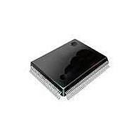
SAA7115HLBE NXP Semiconductors, SAA7115HLBE Datasheet - Page 48

SAA7115HLBE
Manufacturer Part Number
SAA7115HLBE
Description
Video ICs ADV DGTL VIDEO DECODR
Manufacturer
NXP Semiconductors
Datasheet
1.SAA7115HLBE.pdf
(548 pages)
Specifications of SAA7115HLBE
Operating Supply Voltage
3.3 V
Maximum Operating Temperature
+ 70 C
Package / Case
SOT-407
Minimum Operating Temperature
0 C
Mounting Style
SMD/SMT
Number Of Channels
2
Resolution
8 bit
Lead Free Status / RoHS Status
Lead free / RoHS Compliant
Other names
SAA7115HL/V1,557 SAF7115HLBE
- Current page: 48 of 548
- Download datasheet (6Mb)
PNX1300/01/02/11 Data Book
1-22
Figure 1-1. STRG3, STRG5 test load circuit
Figure 1-2. NORM3 test load circuit
Figure 1-3. WEAK5 test load circuit
Output
Figure 1-4. PCI Output Timing Measurement Con-
ditions
Buffer
PNX1300
Output
Output
Buffer
Buffer
PNX1300
PNX1300
Tri-State
Output
Output
Output
Delay
Delay
CLK
pin
30-ohm
pin
pin
PRELIMINARY SPECIFICATION
V_test
T_fval
T_rval
2” true length
2” true length
2” true length
T_off
50-ohm
50-ohm
50-ohm
T_on
V_tfall
V_trise
rise/fall test point
rise/fall test point
rise/fall test point
V_th
V_tl
12 pF
30 pF
15 pF
Figure 1-5. PCI Input Timing Measurement Conditions
Figure 1-6. PCI T
Figure 1-7. PCI T
Figure 1-8. PCI T
Figure 1-9. JTAG Input Timing
TDI, TMS
Input
TCK
CLK
Output
Output
Output
Buffer
Buffer
Buffer
V_th
V_tl
V_test
val
val
val
pin
pin
pin
(max) Rising Edge
(max) Falling Edge
(min) and Slew Rate
1K Ω
T
25 Ω
10 pF
su_TCK
T_su
inputs
valid
Philips Semiconductors
valid
T_h
V_test
1/2 in. max
10 pF
25 Ω
10 pF
1/2 in. max
1/2 in. max
T
V_test
h_TCK
Vcc
1K Ω
V_max
V_th
V_tl
Vcc
Related parts for SAA7115HLBE
Image
Part Number
Description
Manufacturer
Datasheet
Request
R
Part Number:
Description:
Ntsc/pal/secam 9-bit Video Decoder
Manufacturer:
NXP Semiconductors
Datasheet:
Part Number:
Description:
NXP Semiconductors designed the LPC2420/2460 microcontroller around a 16-bit/32-bitARM7TDMI-S CPU core with real-time debug interfaces that include both JTAG andembedded trace
Manufacturer:
NXP Semiconductors
Datasheet:

Part Number:
Description:
NXP Semiconductors designed the LPC2458 microcontroller around a 16-bit/32-bitARM7TDMI-S CPU core with real-time debug interfaces that include both JTAG andembedded trace
Manufacturer:
NXP Semiconductors
Datasheet:
Part Number:
Description:
NXP Semiconductors designed the LPC2468 microcontroller around a 16-bit/32-bitARM7TDMI-S CPU core with real-time debug interfaces that include both JTAG andembedded trace
Manufacturer:
NXP Semiconductors
Datasheet:
Part Number:
Description:
NXP Semiconductors designed the LPC2470 microcontroller, powered by theARM7TDMI-S core, to be a highly integrated microcontroller for a wide range ofapplications that require advanced communications and high quality graphic displays
Manufacturer:
NXP Semiconductors
Datasheet:
Part Number:
Description:
NXP Semiconductors designed the LPC2478 microcontroller, powered by theARM7TDMI-S core, to be a highly integrated microcontroller for a wide range ofapplications that require advanced communications and high quality graphic displays
Manufacturer:
NXP Semiconductors
Datasheet:
Part Number:
Description:
The Philips Semiconductors XA (eXtended Architecture) family of 16-bit single-chip microcontrollers is powerful enough to easily handle the requirements of high performance embedded applications, yet inexpensive enough to compete in the market for hi
Manufacturer:
NXP Semiconductors
Datasheet:
Part Number:
Description:
The XA-S3 device is a member of Philips Semiconductors? XA(eXtended Architecture) family of high performance 16-bitsingle-chip microcontrollers
Manufacturer:
NXP Semiconductors
Datasheet:

Part Number:
Description:
The NXP BlueStreak LH75401/LH75411 family consists of two low-cost 16/32-bit System-on-Chip (SoC) devices
Manufacturer:
NXP Semiconductors
Datasheet:

Part Number:
Description:
The NXP LPC3130/3131 combine an 180 MHz ARM926EJ-S CPU core, high-speed USB2
Manufacturer:
NXP Semiconductors
Datasheet:

Part Number:
Description:
The NXP LPC3141 combine a 270 MHz ARM926EJ-S CPU core, High-speed USB 2
Manufacturer:
NXP Semiconductors

Part Number:
Description:
The NXP LPC3143 combine a 270 MHz ARM926EJ-S CPU core, High-speed USB 2
Manufacturer:
NXP Semiconductors

Part Number:
Description:
The NXP LPC3152 combines an 180 MHz ARM926EJ-S CPU core, High-speed USB 2
Manufacturer:
NXP Semiconductors

Part Number:
Description:
The NXP LPC3154 combines an 180 MHz ARM926EJ-S CPU core, High-speed USB 2
Manufacturer:
NXP Semiconductors


