AOB482L Alpha & Omega Semiconductor Inc, AOB482L Datasheet
AOB482L
Specifications of AOB482L
AOB482


Related parts for AOB482L


AOB482L Summary of contents
Page 1
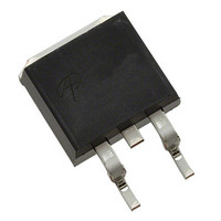
... General Description The AOT482L/AOB482L is fabricated with SDMOS trench technology that combines excellent R gate charge and low Q .The result is outstanding rr efficiency with controlled switching behavior. This universal technology is well suited for PWM, load switching and general purpose applications. TO220 Top View Bottom View ...
Page 2
... Ratings are based on low frequency and duty cycles to keep initial J(MAX) and case to ambient. θJC =175°C. The SOA curve provides a single pulse rating. 2 FR-4 board with 2oz. Copper still air environment with T www.aosmd.com AOT482L/AOB482L Min Typ Max Units =55° ...
Page 3
... Figure 2: Transfer Characteristics (Note E) 2.4 2.2 2 1.8 1.6 1.4 =10V GS 1 1.0E+02 I =20A D 1.0E+01 40 125°C 1.0E+00 1.0E-01 1.0E-02 1.0E-03 1.0E- 0.0 www.aosmd.com AOT482L/AOB482L =5V 125°C 25° (Volts =10V GS I =20A = =20A 100 125 150 175 0 Temperature (°C) 18 Figure 4: On-Resistance vs. Junction Temperature (Note E) 125° ...
Page 4
... DC 10ms 2000 1000 0 10 100 1000 1E-05 0.0001 0.001 Figure 10: Single Pulse Power Rating Junction-to- In descending order D=0.5, 0.3, 0.1, 0.05, 0.02, 0.01, single pulse 40 0.0001 0.001 0.01 Pulse Width (s) www.aosmd.com AOT482L/AOB482L C iss C oss C rss (Volts) DS Figure 8: Capacitance Characteristics T =175°C ...
Page 5
... Figure 13: Power De-rating (Note F) 1000 100 10 1 0.01 125 150 175 Figure 15: Single Pulse Power Rating Junction-to- In descending order D=0.5, 0.3, 0.1, 0.05, 0.02, 0.01, single pulse 40 Single Pulse 1 10 Pulse Width (s) www.aosmd.com AOT482L/AOB482L 50 75 100 125 150 175 T (°C) CASE T =25° ...
Page 6
... Figure 18: Diode Reverse Recovery Time and Softness Factor vs. Conduction Current 25º 25º 800 1000 0 Figure 20: Diode Reverse Recovery Time and www.aosmd.com AOT482L/AOB482L 125ºC 25ºC 25ºC 125º ( =20A s 125º 25ºC 25ºC S 125ºC 200 400 600 800 1000 di/dt (A/µs) Softness Factor vs ...
Page 7
... Vds + DUT Vdd VDC - Vgs t d(on) Unclamped Inductive Switching (UIS) Test Circuit & Waveforms Vds + Vgs Vdd VDC Id - Vgs Diode Recovery Test Circuit & Waveforms Vgs Isd + Vdd VDC - Vds www.aosmd.com AOT482L/AOB482L Qg Qgs Qgd Charge 90% 10 d(off off DSS Idt ...