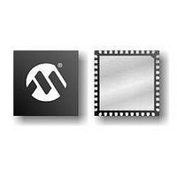
PIC16F1937-E/MV Microchip Technology, PIC16F1937-E/MV Datasheet - Page 190

PIC16F1937-E/MV
Manufacturer Part Number
PIC16F1937-E/MV
Description
14KB Flash, 512B RAM, 256B EEPROM, LCD, 1.8-5.5V 40 UQFN 5x5x0.5mm TUBE
Manufacturer
Microchip Technology
Series
PIC® XLP™ 16Fr
Datasheet
1.PIC16F1937-EMV.pdf
(472 pages)
Specifications of PIC16F1937-E/MV
Processor Series
PIC16F
Core
PIC
Program Memory Type
Flash
Program Memory Size
14 KB
Data Ram Size
256 B
Interface Type
MI2C, SPI, EUSART
Number Of Timers
5
Operating Supply Voltage
1.8 V to 5.5 V
Maximum Operating Temperature
+ 125 C
Mounting Style
SMD/SMT
Package / Case
UQFN-40
Development Tools By Supplier
MPLAB IDE Software
Minimum Operating Temperature
- 40 C
Core Processor
PIC
Core Size
8-Bit
Speed
32MHz
Connectivity
I²C, LIN, SPI, UART/USART
Peripherals
Brown-out Detect/Reset, LCD, POR, PWM, WDT
Number Of I /o
36
Eeprom Size
256 x 8
Ram Size
512 x 8
Voltage - Supply (vcc/vdd)
1.8 V ~ 5.5 V
Data Converters
A/D 14x10b
Oscillator Type
Internal
Operating Temperature
-40°C ~ 125°C
Lead Free Status / Rohs Status
Details
- Current page: 190 of 472
- Download datasheet (5Mb)
PIC16(L)F1934/6/7
REGISTER 19-2:
TABLE 19-2:
DS41364E-page 190
bit 7
Legend:
R = Readable bit
u = Bit is unchanged
‘1’ = Bit is set
bit 7
bit 6
bit 5
bit 4
bit 3
bit 2
bit 1
bit 0
ANSELA
SRCON0
SRCON1
TRISA
Legend: — = unimplemented location, read as ‘0’. Shaded cells are unused by the SR Latch module.
Name
R/W-0/0
SRSPE
TRISA7
SRSPE
SRLEN
SRSPE: SR Latch Peripheral Set Enable bit
1 = SR Latch is set when the SRI pin is high.
0 = SRI pin has no effect on the set input of the SR Latch
SRSCKE: SR Latch Set Clock Enable bit
1 = Set input of SR Latch is pulsed with SRCLK
0 = SRCLK has no effect on the set input of the SR Latch
SRSC2E: SR Latch C2 Set Enable bit
1 = SR Latch is set when the C2 Comparator output is high
0 = C2 Comparator output has no effect on the set input of the SR Latch
SRSC1E: SR Latch C1 Set Enable bit
1 = SR Latch is set when the C1 Comparator output is high
0 = C1 Comparator output has no effect on the set input of the SR Latch
SRRPE: SR Latch Peripheral Reset Enable bit
1 = SR Latch is reset when the SRI pin is high.
0 = SRI pin has no effect on the reset input of the SR Latch
SRRCKE: SR Latch Reset Clock Enable bit
1 = Reset input of SR Latch is pulsed with SRCLK
0 = SRCLK has no effect on the reset input of the SR Latch
SRRC2E: SR Latch C2 Reset Enable bit
1 = SR Latch is reset when the C2 Comparator output is high
0 = C2 Comparator output has no effect on the reset input of the SR Latch
SRRC1E: SR Latch C1 Reset Enable bit
1 = SR Latch is reset when the C1 Comparator output is high
0 = C1 Comparator output has no effect on the reset input of the SR Latch
Bit 7
SUMMARY OF REGISTERS ASSOCIATED WITH SR LATCH MODULE
SRSCKE
—
R/W-0/0
SRCON1: SR LATCH CONTROL 1 REGISTER
SRSCKE
TRISA6
Bit 6
W = Writable bit
x = Bit is unknown
‘0’ = Bit is cleared
—
SRSC2E
R/W-0/0
SRCLK<2:0>
SRSC2E
TRISA5
ANSA5
Bit 5
SRSC1E
R/W-0/0
SRSC1E
TRISA4
ANSA4
Bit 4
U = Unimplemented bit, read as ‘0’
-n/n = Value at POR and BOR/Value at all other Resets
R/W-0/0
SRRPE
SRQEN
SRRPE
TRISA3
ANSA3
Bit 3
SRNQEN
SRRCKE SRRC2E SRRC1E
TRISA2
ANSA2
Bit 2
SRRCKE
R/W-0/0
2008-2011 Microchip Technology Inc.
TRISA1
ANSA1
SRPS
Bit 1
SRRC2E
R/W-0/0
TRISA0
ANSA0
SRPR
Bit 0
SRRC1E
R/W-0/0
Register
on Page
134
189
190
133
bit 0
Related parts for PIC16F1937-E/MV
Image
Part Number
Description
Manufacturer
Datasheet
Request
R

Part Number:
Description:
IC, 8BIT MCU, PIC16F, 32MHZ, SOIC-18
Manufacturer:
Microchip Technology
Datasheet:

Part Number:
Description:
IC, 8BIT MCU, PIC16F, 32MHZ, SSOP-20
Manufacturer:
Microchip Technology
Datasheet:

Part Number:
Description:
IC, 8BIT MCU, PIC16F, 32MHZ, DIP-18
Manufacturer:
Microchip Technology
Datasheet:

Part Number:
Description:
IC, 8BIT MCU, PIC16F, 32MHZ, QFN-28
Manufacturer:
Microchip Technology
Datasheet:

Part Number:
Description:
IC, 8BIT MCU, PIC16F, 32MHZ, QFN-28
Manufacturer:
Microchip Technology
Datasheet:

Part Number:
Description:
IC, 8BIT MCU, PIC16F, 32MHZ, QFN-28
Manufacturer:
Microchip Technology
Datasheet:

Part Number:
Description:
IC, 8BIT MCU, PIC16F, 32MHZ, SSOP-20
Manufacturer:
Microchip Technology
Datasheet:

Part Number:
Description:
IC, 8BIT MCU, PIC16F, 20MHZ, DIP-40
Manufacturer:
Microchip Technology
Datasheet:

Part Number:
Description:
IC, 8BIT MCU, PIC16F, 32MHZ, QFN-28
Manufacturer:
Microchip Technology
Datasheet:

Part Number:
Description:
IC, 8BIT MCU, PIC16F, 20MHZ, MQFP-44
Manufacturer:
Microchip Technology
Datasheet:

Part Number:
Description:
IC, 8BIT MCU, PIC16F, 20MHZ, QFN-20
Manufacturer:
Microchip Technology
Datasheet:

Part Number:
Description:
IC, 8BIT MCU, PIC16F, 32MHZ, QFN-28
Manufacturer:
Microchip Technology
Datasheet:

Part Number:
Description:
MCU 14KB FLASH 768B RAM 64-TQFP
Manufacturer:
Microchip Technology
Datasheet:

Part Number:
Description:
7 KB Flash, 384 Bytes RAM, 32 MHz Int. Osc, 16 I/0, Enhanced Mid Range Core, Low
Manufacturer:
Microchip Technology

Part Number:
Description:
14KB Flash, 512B RAM, 256B EEPROM, LCD, 1.8-5.5V 40 UQFN 5x5x0.5mm TUBE
Manufacturer:
Microchip Technology


