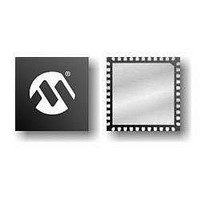
PIC16F1937-E/MV Microchip Technology, PIC16F1937-E/MV Datasheet - Page 344

PIC16F1937-E/MV
Manufacturer Part Number
PIC16F1937-E/MV
Description
14KB Flash, 512B RAM, 256B EEPROM, LCD, 1.8-5.5V 40 UQFN 5x5x0.5mm TUBE
Manufacturer
Microchip Technology
Series
PIC® XLP™ 16Fr
Datasheet
1.PIC16F1937-EMV.pdf
(472 pages)
Specifications of PIC16F1937-E/MV
Processor Series
PIC16F
Core
PIC
Program Memory Type
Flash
Program Memory Size
14 KB
Data Ram Size
256 B
Interface Type
MI2C, SPI, EUSART
Number Of Timers
5
Operating Supply Voltage
1.8 V to 5.5 V
Maximum Operating Temperature
+ 125 C
Mounting Style
SMD/SMT
Package / Case
UQFN-40
Development Tools By Supplier
MPLAB IDE Software
Minimum Operating Temperature
- 40 C
Core Processor
PIC
Core Size
8-Bit
Speed
32MHz
Connectivity
I²C, LIN, SPI, UART/USART
Peripherals
Brown-out Detect/Reset, LCD, POR, PWM, WDT
Number Of I /o
36
Eeprom Size
256 x 8
Ram Size
512 x 8
Voltage - Supply (vcc/vdd)
1.8 V ~ 5.5 V
Data Converters
A/D 14x10b
Oscillator Type
Internal
Operating Temperature
-40°C ~ 125°C
Lead Free Status / Rohs Status
Details
- Current page: 344 of 472
- Download datasheet (5Mb)
PIC16(L)F1934/6/7
27.9
LCD waveforms are generated so that the net AC
voltage across the dark pixel should be maximized and
the net AC voltage across the clear pixel should be
minimized. The net DC voltage across any pixel should
be zero.
The COM signal represents the time slice for each
common, while the SEG contains the pixel data.
The pixel signal (COM-SEG) will have no DC
component and it can take only one of the two RMS
values. The higher RMS value will create a dark pixel
and a lower RMS value will create a clear pixel.
As the number of commons increases, the delta
between the two RMS values decreases. The delta
represents the maximum contrast that the display can
have.
FIGURE 27-8:
DS41364E-page 344
COM0
LCD Waveform Generation
TYPE-A/TYPE-B WAVEFORMS IN STATIC DRIVE
segment voltage
segment voltage
COM0-SEG0
COM0-SEG1
COM0 pin
SEG0 pin
SEG1 pin
(inactive)
(active)
The LCDs can be driven by two types of waveform:
Type-A and Type-B. In Type-A waveform, the phase
changes within each common type, whereas in Type-B
waveform, the phase changes on each frame
boundary. Thus, Type-A waveform maintains 0 V
over a single frame, whereas Type-B waveform takes
two frames.
Figure 27-8
for static, half-multiplex, 1/3-multiplex and 1/4-multiplex
drives for Type-A and Type-B waveforms.
Note 1: If Sleep has to be executed with LCD
1 Frame
2: When the LCD clock source is F
Sleep disabled (LCDCON<SLPEN> is
‘1’), then care must be taken to execute
Sleep only when V
‘0’.
if Sleep is executed, irrespective of the
LCDCON<SLPEN> setting, the LCD
immediately goes into Sleep. Thus, take
care to see that V
when Sleep is executed.
through
2008-2011 Microchip Technology Inc.
Figure 27-18
DC
DC
on all the pixels is
on all pixels is ‘0’
provide waveforms
OSC
V
V
V
V
V
V
V
V
-V
V
/256,
1
0
1
0
1
0
1
0
0
1
DC
Related parts for PIC16F1937-E/MV
Image
Part Number
Description
Manufacturer
Datasheet
Request
R

Part Number:
Description:
IC, 8BIT MCU, PIC16F, 32MHZ, SOIC-18
Manufacturer:
Microchip Technology
Datasheet:

Part Number:
Description:
IC, 8BIT MCU, PIC16F, 32MHZ, SSOP-20
Manufacturer:
Microchip Technology
Datasheet:

Part Number:
Description:
IC, 8BIT MCU, PIC16F, 32MHZ, DIP-18
Manufacturer:
Microchip Technology
Datasheet:

Part Number:
Description:
IC, 8BIT MCU, PIC16F, 32MHZ, QFN-28
Manufacturer:
Microchip Technology
Datasheet:

Part Number:
Description:
IC, 8BIT MCU, PIC16F, 32MHZ, QFN-28
Manufacturer:
Microchip Technology
Datasheet:

Part Number:
Description:
IC, 8BIT MCU, PIC16F, 32MHZ, QFN-28
Manufacturer:
Microchip Technology
Datasheet:

Part Number:
Description:
IC, 8BIT MCU, PIC16F, 32MHZ, SSOP-20
Manufacturer:
Microchip Technology
Datasheet:

Part Number:
Description:
IC, 8BIT MCU, PIC16F, 20MHZ, DIP-40
Manufacturer:
Microchip Technology
Datasheet:

Part Number:
Description:
IC, 8BIT MCU, PIC16F, 32MHZ, QFN-28
Manufacturer:
Microchip Technology
Datasheet:

Part Number:
Description:
IC, 8BIT MCU, PIC16F, 20MHZ, MQFP-44
Manufacturer:
Microchip Technology
Datasheet:

Part Number:
Description:
IC, 8BIT MCU, PIC16F, 20MHZ, QFN-20
Manufacturer:
Microchip Technology
Datasheet:

Part Number:
Description:
IC, 8BIT MCU, PIC16F, 32MHZ, QFN-28
Manufacturer:
Microchip Technology
Datasheet:

Part Number:
Description:
MCU 14KB FLASH 768B RAM 64-TQFP
Manufacturer:
Microchip Technology
Datasheet:

Part Number:
Description:
7 KB Flash, 384 Bytes RAM, 32 MHz Int. Osc, 16 I/0, Enhanced Mid Range Core, Low
Manufacturer:
Microchip Technology

Part Number:
Description:
14KB Flash, 512B RAM, 256B EEPROM, LCD, 1.8-5.5V 40 UQFN 5x5x0.5mm TUBE
Manufacturer:
Microchip Technology


