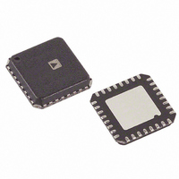
AD9515BCPZ Analog Devices Inc, AD9515BCPZ Datasheet - Page 18

AD9515BCPZ
Manufacturer Part Number
AD9515BCPZ
Description
IC CLOCK DIST 2OUT PLL 32LFCSP
Manufacturer
Analog Devices Inc
Type
Fanout Buffer (Distribution), Dividerr
Datasheet
1.AD9515BCPZ.pdf
(28 pages)
Specifications of AD9515BCPZ
Design Resources
Low Jitter Sampling Clock Generator for High Performance ADCs Using AD9958/9858 and AD9515 (CN0109)
Number Of Circuits
1
Ratio - Input:output
1:2
Differential - Input:output
Yes/Yes
Input
Differential
Output
CMOS, LVDS, LVPECL
Frequency - Max
1.6GHz
Voltage - Supply
3.135 V ~ 3.465 V
Operating Temperature
-40°C ~ 85°C
Mounting Type
Surface Mount
Package / Case
32-LFCSP
Frequency-max
1.6GHz
No. Of Multipliers / Dividers
2
No. Of Amplifiers
3
Supply Voltage Range
3.135V To 3.465V
Slew Rate
1V/ns
Operating Temperature Range
-40°C To +85°C
Digital Ic Case Style
LFCSP
Lead Free Status / RoHS Status
Lead free / RoHS Compliant
For Use With
AD9515/PCBZ - BOARD EVAL CLOCK 2CH AD9515
Lead Free Status / RoHS Status
Lead free / RoHS Compliant, Lead free / RoHS Compliant
Available stocks
Company
Part Number
Manufacturer
Quantity
Price
Company:
Part Number:
AD9515BCPZ
Manufacturer:
ADI
Quantity:
142
Part Number:
AD9515BCPZ
Manufacturer:
ADI/亚德诺
Quantity:
20 000
AD9515
FUNCTIONAL DESCRIPTION
OVERALL
The AD9515 provides for the distribution of its input clock on
one or both of its outputs. OUT0 is an LVPECL output. OUT1
can be set to either LVDS or CMOS logic levels. Each output
has its own divider that can be set for a divide ratio selected
from a list of integer values from 1 (bypassed) to 32.
OUT1 includes an analog delay block that can be set to add an
additional delay of 1.5 ns, 5 ns, or 10 ns full scale, each with
16 levels of fine adjustment.
CLK, CLKB—DIFFERENTIAL CLOCK INPUT
The CLK and CLKB pins are differential clock input pins.
This input works up to 1600 MHz. The jitter performance is
degraded by a slew rate below 1 V/ns. The input level should be
between approximately 150 mV p-p to no more than 2 V p-p.
Anything greater can result in turning on the protection diodes
on the input pins.
See Figure 23 for the CLK equivalent input circuit. This
input is fully differential and self-biased. The signal should be
ac-coupled using capacitors. If a single-ended input must be
used, this can be accommodated by ac coupling to one side of
the differential input only. The other side of the input should be
bypassed to a quiet ac ground by a capacitor.
SYNCHRONIZATION
Power-On SYNC
A power-on sync (POS) is issued when the V
turned on to ensure that the outputs start in synchronization.
The power-on sync works only if the V
tions the region from 2.2 V to 3.1 V within 35 ms. The POS can
occur up to 65 ms after V
not divide = 1 are synchronized.
CLKB
CLK
V
S
Figure 23. Clock Input Equivalent Circuit
5kΩ
5kΩ
2.5kΩ
S
crosses 2.2 V. Only outputs which are
2.5kΩ
CLOCK INPUT
S
power supply transi-
STAGE
S
power supply is
Rev. 0 | Page 18 of 28
OUT
SYNCB
If the setup configuration of the AD9515 is changed during
operation, the outputs can become unsynchronized. The
outputs can be re-synchronized to each other at any time.
Synchronization occurs when the SYNCB pin is pulled low and
released. The clock outputs (except where divide = 1) are forced
into a fixed state (determined by the divide and phase settings)
and held there in a static condition, until the SYNCB pin is
returned to high. Upon release of the SYNCB pin, after four
cycles of the clock signal at CLK, all outputs continue clocking
in synchronicity (except where divide = 1).
When divide = 1 for an output, that output is not affected by
SYNCB.
SYNCB
SYNCB
The outputs of the AD9515 can be synchronized by using the
SYNCB pin. Synchronization aligns the phases of the clock
outputs, respecting any phase offset that has been set on an
output’s divider.
CLK
V
CLK
OUT
OUT
CLK
S
INTERNAL SYNC NODE
DEPENDS ON PREVIOUS STATE
0V
EXAMPLE: DIVIDE ≥ 8
PHASE = 0
DIVIDE = 2
PHASE = 0
CLOCK FREQUENCY
IS EXAMPLE ONLY
Figure 26. SYNCB Timing with No Clock Present
3 CLK CYCLES
MIN 5ns
Figure 25. SYNCB Timing with Clock Present
Figure 27. SYNCB Equivalent Input Circuit
Figure 24. Power-On Sync Timing
§
2.2V
SYNCB
DEPENDS ON PREVIOUS STATE AND DIVIDE RATIO
§
4 CLK CYCLES
§
35ms
MAX
3.1V
4 CLK CYCLES
< 65ms
§
3.3V
EXAMPLE DIVIDE
RATIO PHASE = 0
EXAMPLE DIVIDE
RATIO PHASE = 0


