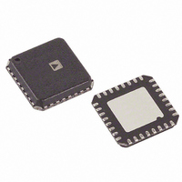
AD9515BCPZ Analog Devices Inc, AD9515BCPZ Datasheet - Page 20

AD9515BCPZ
Manufacturer Part Number
AD9515BCPZ
Description
IC CLOCK DIST 2OUT PLL 32LFCSP
Manufacturer
Analog Devices Inc
Type
Fanout Buffer (Distribution), Dividerr
Datasheet
1.AD9515BCPZ.pdf
(28 pages)
Specifications of AD9515BCPZ
Design Resources
Low Jitter Sampling Clock Generator for High Performance ADCs Using AD9958/9858 and AD9515 (CN0109)
Number Of Circuits
1
Ratio - Input:output
1:2
Differential - Input:output
Yes/Yes
Input
Differential
Output
CMOS, LVDS, LVPECL
Frequency - Max
1.6GHz
Voltage - Supply
3.135 V ~ 3.465 V
Operating Temperature
-40°C ~ 85°C
Mounting Type
Surface Mount
Package / Case
32-LFCSP
Frequency-max
1.6GHz
No. Of Multipliers / Dividers
2
No. Of Amplifiers
3
Supply Voltage Range
3.135V To 3.465V
Slew Rate
1V/ns
Operating Temperature Range
-40°C To +85°C
Digital Ic Case Style
LFCSP
Lead Free Status / RoHS Status
Lead free / RoHS Compliant
For Use With
AD9515/PCBZ - BOARD EVAL CLOCK 2CH AD9515
Lead Free Status / RoHS Status
Lead free / RoHS Compliant, Lead free / RoHS Compliant
Available stocks
Company
Part Number
Manufacturer
Quantity
Price
Company:
Part Number:
AD9515BCPZ
Manufacturer:
ADI
Quantity:
142
Part Number:
AD9515BCPZ
Manufacturer:
ADI/亚德诺
Quantity:
20 000
AD9515
PROGRAMMING
Table 10. S0—OUT1 Delay Full Scale
S0
0
1/3
2/3
1
Table 11. S1—Output Logic Configuration
S1
0
1/3
2/3
1
Table 12. S2, S3, and S4—OUT0
S2
0
1/3
2/3
1
0
1/3
2/3
1
0
1/3
2/3
1
0
1/3
2/3
1
0
1/3
2/3
1
0
1/3
2/3
1
0
S3
0
0
0
0
1/3
1/3
1/3
1/3
2/3
2/3
2/3
2/3
1
1
1
1
0
0
0
0
1/3
1/3
1/3
1/3
2/3
Delay
Bypassed
1.5 ns
5 ns
10 ns
OUT0
LVPECL 790 mV
LVPECL 400 mV
LVPECL 790 mV
LVPECL 400 mV
S4
0
0
1/3
1/3
0
0
0
0
0
0
0
0
0
0
0
0
0
0
1/3
1/3
1/3
1/3
1/3
1/3
1/3
OUT0
Divide (Duty Cycle
1
2 (50%)
3 (33%)
4 (50%)
5 (40%)
6 (50%)
7 (43%)
8 (50%)
9 (44%)
10 (50%)
11 (45%)
12 (50%)
OUT0 OFF
14 (50%)
15 (47%)
16 (50%)
17 (47%)
18 (50%)
19 (47%)
20 (50%)
21 (48%)
22 (50%)
23 (48%)
24 (50%)
25 (48%)
OUT1
LVDS
LVDS
CMOS
CMOS
1
)
OUT0
Phase
0
0
0
0
0
0
0
0
0
0
0
0
0
0
0
0
0
0
0
0
0
0
0
0
Rev. 0 | Page 20 of 28
S2
1/3
2/3
1
0
1/3
2/3
1
0
1/3
2/3
1
0
1/3
2/3
1
0
1/3
2/3
1
0
1/3
2/3
1
0
1/3
2/3
1
0
1/3
2/3
1
0
1/3
2/3
1
0
1/3
2/3
1
1
Duty cycle is the clock signal high time divided by the total period.
S3
2/3
2/3
2/3
1
1
1
1
0
0
0
0
1/3
1/3
1/3
1/3
2/3
2/3
2/3
2/3
1
1
1
1
0
0
0
0
1/3
1/3
1/3
1/3
2/3
2/3
2/3
2/3
1
1
1
1
S4
1/3
1/3
1/3
1/3
1/3
1/3
1/3
2/3
2/3
2/3
2/3
2/3
2/3
2/3
2/3
2/3
2/3
2/3
2/3
2/3
2/3
2/3
2/3
1
1
1
1
1
1
1
1
1
1
1
1
1
1
1
1
OUT0
Divide (Duty Cycle
26 (50%)
27 (48%)
28 (50%)
29 (48%)
30 (50%)
31 (48%)
32 (50%)
2 (50%)
4 (50%)
4 (50%)
4 (50%)
8 (50%)
8 (50%)
8 (50%)
8 (50%)
8 (50%)
8 (50%)
8 (50%)
16 (50%)
16 (50%)
16 (50%)
16 (50%)
16 (50%)
16 (50%)
16 (50%)
16 (50%)
16 (50%)
16 (50%)
16 (50%)
16 (50%)
16 (50%)
16 (50%)
16 (50%)
32 (50%)
32 (50%)
32 (50%)
32 (50%)
32 (50%)
Do not use
1
)
OUT0
Phase
0
0
0
0
0
0
0
1
1
2
3
1
2
3
4
5
6
7
1
2
3
4
5
6
7
8
9
10
11
12
13
14
15
1
2
3
4
5


