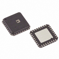
AD9515BCPZ Analog Devices Inc, AD9515BCPZ Datasheet - Page 4

AD9515BCPZ
Manufacturer Part Number
AD9515BCPZ
Description
IC CLOCK DIST 2OUT PLL 32LFCSP
Manufacturer
Analog Devices Inc
Type
Fanout Buffer (Distribution), Dividerr
Datasheet
1.AD9515BCPZ.pdf
(28 pages)
Specifications of AD9515BCPZ
Design Resources
Low Jitter Sampling Clock Generator for High Performance ADCs Using AD9958/9858 and AD9515 (CN0109)
Number Of Circuits
1
Ratio - Input:output
1:2
Differential - Input:output
Yes/Yes
Input
Differential
Output
CMOS, LVDS, LVPECL
Frequency - Max
1.6GHz
Voltage - Supply
3.135 V ~ 3.465 V
Operating Temperature
-40°C ~ 85°C
Mounting Type
Surface Mount
Package / Case
32-LFCSP
Frequency-max
1.6GHz
No. Of Multipliers / Dividers
2
No. Of Amplifiers
3
Supply Voltage Range
3.135V To 3.465V
Slew Rate
1V/ns
Operating Temperature Range
-40°C To +85°C
Digital Ic Case Style
LFCSP
Lead Free Status / RoHS Status
Lead free / RoHS Compliant
For Use With
AD9515/PCBZ - BOARD EVAL CLOCK 2CH AD9515
Lead Free Status / RoHS Status
Lead free / RoHS Compliant, Lead free / RoHS Compliant
Available stocks
Company
Part Number
Manufacturer
Quantity
Price
Company:
Part Number:
AD9515BCPZ
Manufacturer:
ADI
Quantity:
142
Part Number:
AD9515BCPZ
Manufacturer:
ADI/亚德诺
Quantity:
20 000
AD9515
TIMING CHARACTERISTICS
CLK input slew rate = 1 V/ns or greater.
Table 3.
Parameter
LVPECL
PROPAGATION DELAY, t
OUTPUT SKEW, LVPECL OUTPUT
LVDS
PROPAGATION DELAY, t
OUTPUT SKEW, LVDS OUTPUT
PROPAGATION DELAY, t
OUTPUT SKEW, CMOS OUTPUT
LVPECL-TO-CMOS OUT
DELAY ADJUST (OUT2; LVDS AND CMOS)
Output Rise Time, t
Output Fall Time, t
Divide = 1
Divide = 2 − 32
Variation with Temperature
LVPECL OUT Across Multiple Parts, t
Output Rise Time, t
Output Fall Time, t
OUT3 to OUT4
Divide = 1
Divide = 2 − 32
Variation with Temperature
LVDS OUT Across Multiple Parts, t
CMOS
Output Rise Time, t
Output Fall Time, t
Divide = 1
Divide = 2 − 32
Variation with Temperature
CMOS OUT Across Multiple Parts, t
LVPECL-TO-LVDS OUT
Output Delay, t
Output Delay, t
S0 = 1/3
S0 = 2/3
Zero Scale Delay Time
Full Scale Time Delay
Zero Scale Delay Time
Full Scale Time Delay
Zero Scale Variation with Temperature
Full Scale Variation with Temperature
Zero Scale Variation with Temperature
Full Scale Variation with Temperature
SKP_V
SKP_C
FP
FL
FC
RP
RL
RC
PECL
LVDS
CMOS
2
2
2
2
, CLK-TO-LVPECL OUT
, CLK-TO-LVDS OUT
, CLK-TO-CMOS OUT
SKV_AB
SKC_AB
SKP_AB3
1
1
1
Min
355
395
1.00
1.05
1.10
1.15
700
0.88
Rev. 0 | Page 4 of 28
Typ
60
60
480
530
0.5
200
210
1.25
1.30
0.9
650
650
1.45
1.50
1
970
1.14
0.34
0.20
1.7
−0.38
0.45
0.31
5.9
−1.3
Max
100
100
635
710
125
350
350
1.55
1.60
230
865
990
1.75
1.80
300
1150
1.43
Unit
ps
ps
ps
ps
ps/°C
ps
ps
ps
ns
ns
ps/°C
ps
ps
ps
ns
ns
ps/°C
ps
ps
ns
ns
ps/°C
ns
ps/°C
ns
ps/°C
ns
ps/°C
Test Conditions/Comments
Termination = 50 Ω to V
20% to 80%, measured differentially
80% to 20%, measured differentially
Termination = 100 Ω differential
20% to 80%, measured differentially
80% to 20%, measured differentially
Delay off on OUT4
Delay off on OUT4
B outputs are inverted; termination = open
20% to 80%; C
80% to 20%; C
Delay off on OUT4
Delay off on OUT4
Everything the same; different logic type
LVPECL to LVDS on same part
Everything the same; different logic type
LVPECL to CMOS on same part
LOAD
LOAD
= 3 pF
= 3 pF
S
− 2 V


