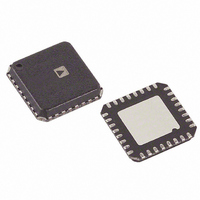
AD9515BCPZ Analog Devices Inc, AD9515BCPZ Datasheet - Page 23

AD9515BCPZ
Manufacturer Part Number
AD9515BCPZ
Description
IC CLOCK DIST 2OUT PLL 32LFCSP
Manufacturer
Analog Devices Inc
Type
Fanout Buffer (Distribution), Dividerr
Datasheet
1.AD9515BCPZ.pdf
(28 pages)
Specifications of AD9515BCPZ
Design Resources
Low Jitter Sampling Clock Generator for High Performance ADCs Using AD9958/9858 and AD9515 (CN0109)
Number Of Circuits
1
Ratio - Input:output
1:2
Differential - Input:output
Yes/Yes
Input
Differential
Output
CMOS, LVDS, LVPECL
Frequency - Max
1.6GHz
Voltage - Supply
3.135 V ~ 3.465 V
Operating Temperature
-40°C ~ 85°C
Mounting Type
Surface Mount
Package / Case
32-LFCSP
Frequency-max
1.6GHz
No. Of Multipliers / Dividers
2
No. Of Amplifiers
3
Supply Voltage Range
3.135V To 3.465V
Slew Rate
1V/ns
Operating Temperature Range
-40°C To +85°C
Digital Ic Case Style
LFCSP
Lead Free Status / RoHS Status
Lead free / RoHS Compliant
For Use With
AD9515/PCBZ - BOARD EVAL CLOCK 2CH AD9515
Lead Free Status / RoHS Status
Lead free / RoHS Compliant, Lead free / RoHS Compliant
Available stocks
Company
Part Number
Manufacturer
Quantity
Price
Company:
Part Number:
AD9515BCPZ
Manufacturer:
ADI
Quantity:
142
Part Number:
AD9515BCPZ
Manufacturer:
ADI/亚德诺
Quantity:
20 000
When the delay block is OFF (bypassed), it is also powered
down.
OUTPUTS
The AD9515 offers three different output level choices:
LVPECL, LVDS, and CMOS. OUT0/OUT0B offers an LVPECL
differential output. The LVPECL differential voltage swing
(V
OUT1/OUT1B can be selected as either an LVDS differential
output or a pair of CMOS single-ended outputs. If selected as
CMOS, OUT1 is a noninverted, single-ended output, and
OUT1B is an inverted, single-ended output.
OD
) can be selected as either 400 mV or 790 mV (see Table 11).
Figure 31. LVPECL Output Simplified Equivalent Circuit
Figure 32. LVDS Output Simplified Equivalent Circuit
Figure 33. CMOS Equivalent Output Circuit
3.5mA
3.5mA
GND
V
S
3.3V
OUT1/
OUT1B
OUT
OUTB
OUT
OUTB
Rev. 0 | Page 23 of 28
POWER SUPPLY
The AD9515 requires a 3.3 V ± 5% power supply for V
tables in the Specifications section give the performance
expected from the AD9515 with the power supply voltage
within this range. In no case should the absolute maximum
range of −0.3 V to +3.6 V, with respect to GND, be exceeded
on Pin VS.
Good engineering practice should be followed in the layout of
power supply traces and the ground plane of the PCB. The
power supply should be bypassed on the PCB with adequate
capacitance (>10 μF). The AD9515 should be bypassed with
adequate capacitors (0.1 μF) at all power pins as close as
possible to the part. The layout of the AD9515 evaluation
board (AD9515/PCB) is a good example.
AD9515
S
. The


