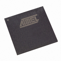
AT94S40AL-25DGC Atmel, AT94S40AL-25DGC Datasheet - Page 10

AT94S40AL-25DGC
Manufacturer Part Number
AT94S40AL-25DGC
Description
IC FPSLIC 40K GATE 25MHZ 256BGA
Manufacturer
Atmel
Series
FPSLIC®r
Datasheet
1.AT94S10AL-25DGC.pdf
(32 pages)
Specifications of AT94S40AL-25DGC
Core Type
8-bit AVR
Speed
16MHz
Interface
I²C, UART
Program Sram Bytes
20K-32K
Fpga Sram
18kb
Eeprom Size
1M x 8
Data Sram Bytes
4K ~ 16K
Fpga Core Cells
2304
Fpga Gates
40K
Fpga Registers
2862
Voltage - Supply
3 V ~ 3.6 V
Mounting Type
Surface Mount
Operating Temperature
0°C ~ 70°C
Package / Case
256-CABGA
Lead Free Status / RoHS Status
Contains lead / RoHS non-compliant
Available stocks
Company
Part Number
Manufacturer
Quantity
Price
4.9.3
4.9.4
4.9.4.1
10
LSB
D0
1st
AT94S Secure Family
Data Byte
Writing
Write Polling
2nd
D1
The organization of the Data Byte is shown above. Note that in this case, the Data Byte is
clocked into the device LSB first and MSB last.
Writing to the normal address space takes place in pages. A page is 128-bytes long in the 1-Mbit
part. The page boundaries are, respectively, addresses where A
and A
of bytes written must be 128 for the 1-Mbit part. The first byte is written at the transmitted
address. The address is incremented in the Configurator following the receipt of each Data Byte.
Only the lower 7 bits of the address are incremented. Thus, after writing to the last byte address
within the given page, the address will roll over to the first byte address of the same page. A
Write Instruction consists of:
On receipt of the Stop Condition, the Configurator enters an internally-timed write cycle. While
the Configurator is busy with this write cycle, it will not acknowledge any transfers. The program-
mer can start the next page write by sending the Start Condition followed by the Device Address,
in effect polling the Configurator. If this is not acknowledged, then the programmer should aban-
don the transfer without asserting a Stop Condition. The programmer can then repeatedly
initiate a write instruction as above, until an acknowledge is received. When the Acknowledge
Bit is received, the write instruction should continue by sending the first EEPROM Address Byte
to the Configurator.
An alternative to write polling would be to wait a period of t
data or exiting the programming mode. All signals must be maintained during the entire write
cycle.
E6
a Start Condition
a Device Address Byte with R/W = 0
MS Byte of the EEPROM Address
Next Byte of the EEPROM Address
LS Byte of EEPROM Address
One or more Data Bytes (sent to the
Configurator)
a Stop Condition
down to A
An Acknowledge Bit from the Configurator
An Acknowledge Bit from the Configurator
An Acknowledge Bit from the Configurator
An Acknowledge Bit from the Configurator
Each followed by an Acknowledge Bit from the
Configurator
3rd
D2
E0
are all zero. Writing can start at any address within a page and the number
4th
D3
5th
D4
6th
D5
WR
before sending the next page of
E0
down to A
7th
D6
EOS
2314E–FPSLI–6/05
are all zero,
MSB
D7
8th


