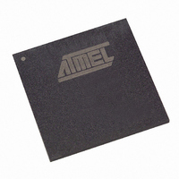
AT94S40AL-25DGC Atmel, AT94S40AL-25DGC Datasheet - Page 6

AT94S40AL-25DGC
Manufacturer Part Number
AT94S40AL-25DGC
Description
IC FPSLIC 40K GATE 25MHZ 256BGA
Manufacturer
Atmel
Series
FPSLIC®r
Datasheet
1.AT94S10AL-25DGC.pdf
(32 pages)
Specifications of AT94S40AL-25DGC
Core Type
8-bit AVR
Speed
16MHz
Interface
I²C, UART
Program Sram Bytes
20K-32K
Fpga Sram
18kb
Eeprom Size
1M x 8
Data Sram Bytes
4K ~ 16K
Fpga Core Cells
2304
Fpga Gates
40K
Fpga Registers
2862
Voltage - Supply
3 V ~ 3.6 V
Mounting Type
Surface Mount
Operating Temperature
0°C ~ 70°C
Package / Case
256-CABGA
Lead Free Status / RoHS Status
Contains lead / RoHS non-compliant
Available stocks
Company
Part Number
Manufacturer
Quantity
Price
4.5
4.6
4.7
Figure 4-1.
Table 4-1.
6
cSCK
cSDA
Where:R/W=1 Read
MSB
1st
1
Acknowledge Bit
Bit Ordering Protocol
Device Address Byte
AT94S Secure Family
= 0 Write
Start and Stop Conditions
Device Address Byte
Byte n
2nd
0
The Acknowledge (ACK) Bit shown in
byte. The receiving Configurator can accept the byte by asserting a Low value on the cSDA line,
or it can refuse the byte by asserting (allowing the signal to be externally pulled up to) a High
value on the cSDA line. All bytes from accepted messages must be terminated by either an
Acknowledge Bit or a Stop Condition. Following an ACK Bit, when the cSDA line is released dur-
ing an exchange of control between the Configurator and the programmer, the cSDA line may
be pulled High temporarily due to the open-collector output nature of the line. Control of the line
must resume before the next rising edge of the clock.
The most significant bit is the first bit of a byte transmitted on the cSDA line for the Device
Address Byte and the EEPROM Address Bytes. It is followed by the lesser significant bits until
the eighth bit, the least significant bit, is transmitted. However, for Data Bytes (both writing and
reading), the first bit transmitted is the least significant bit. This protocol is shown in the diagrams
below.
The contents of the Device Address Byte are shown below, along with the order in which the bits
are clocked into the device.
The CE pin cannot be used for device selection in programming mode (i.e., when SER_EN is
drive Low).
8th Bit
3rd
1
ACK BIT
Condition
4th
STOP
0
Figure 4-1
5th
0
t WR
is provided by the Configurator receiving the
6th
1
Condition
START
7th
1
2314E–FPSLI–6/05
LSB
R/W
8th


