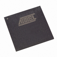
AT94S40AL-25DGC Atmel, AT94S40AL-25DGC Datasheet - Page 3

AT94S40AL-25DGC
Manufacturer Part Number
AT94S40AL-25DGC
Description
IC FPSLIC 40K GATE 25MHZ 256BGA
Manufacturer
Atmel
Series
FPSLIC®r
Datasheet
1.AT94S10AL-25DGC.pdf
(32 pages)
Specifications of AT94S40AL-25DGC
Core Type
8-bit AVR
Speed
16MHz
Interface
I²C, UART
Program Sram Bytes
20K-32K
Fpga Sram
18kb
Eeprom Size
1M x 8
Data Sram Bytes
4K ~ 16K
Fpga Core Cells
2304
Fpga Gates
40K
Fpga Registers
2862
Voltage - Supply
3 V ~ 3.6 V
Mounting Type
Surface Mount
Operating Temperature
0°C ~ 70°C
Package / Case
256-CABGA
Lead Free Status / RoHS Status
Contains lead / RoHS non-compliant
Available stocks
Company
Part Number
Manufacturer
Quantity
Price
Figure 1-1.
2314E–FPSLI–6/05
Configuration Logic
Configuration
EEPROM
and Chip
For ISP
Erase
I/O
AT94S Architecture
The embedded AVR core achieves throughputs approaching 1 MIPS per MHz by executing
powerful instructions in a single-clock-cycle, and allows system designers to optimize power
consumption versus processing speed. The AVR core is based on an enhanced RISC architec-
ture that combines a rich instruction set with 32 general-purpose working registers. All 32
registers are directly connected to the Arithmetic Logic Unit (ALU), allowing two independent
registers to be accessed in one single instruction executed in one clock cycle. The resulting
architecture is more code-efficient while achieving throughputs up to ten times faster than con-
ventional CISC microcontrollers at the same clock frequency. The AVR executes out of on-chip
SRAM. Both the FPGA configuration SRAM and AVR instruction code SRAM are automatically
loaded at system power-up using Atmel’s in-system programmable AT17 Series EEPROM con-
figuration memories, which are part of the AT94S Multi-chip Module (MCM).
State-of-the-art FPSLIC design tools, System Designer, were developed in conjunction with the
FPSLIC architecture to help reduce overall time-to-market by integrating microcontroller devel-
opment and debugging, FPGA development, place and route, and complete system
co-verification in one easy-to-use software tool.
SRAM Memory
Up to 16K x 16
Program
Address Lines
Decoded
Up to 16
5 - 40K Gates FPGA
PROGRAMMABLE I/O
Multiply
16K x 8
SRAM
Up to
with
Data
AT94S Secure Family
Timer/Counters
16 Prog. I/O
2-wire Serial
Two Serial
Two 8-bit
UARTs
Lines
Unit
4 Interrupt Lines
I/O
I/O
I/O
3


