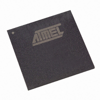
AT94S40AL-25DGC Atmel, AT94S40AL-25DGC Datasheet - Page 4

AT94S40AL-25DGC
Manufacturer Part Number
AT94S40AL-25DGC
Description
IC FPSLIC 40K GATE 25MHZ 256BGA
Manufacturer
Atmel
Series
FPSLIC®r
Datasheet
1.AT94S10AL-25DGC.pdf
(32 pages)
Specifications of AT94S40AL-25DGC
Core Type
8-bit AVR
Speed
16MHz
Interface
I²C, UART
Program Sram Bytes
20K-32K
Fpga Sram
18kb
Eeprom Size
1M x 8
Data Sram Bytes
4K ~ 16K
Fpga Core Cells
2304
Fpga Gates
40K
Fpga Registers
2862
Voltage - Supply
3 V ~ 3.6 V
Mounting Type
Surface Mount
Operating Temperature
0°C ~ 70°C
Package / Case
256-CABGA
Lead Free Status / RoHS Status
Contains lead / RoHS non-compliant
Available stocks
Company
Part Number
Manufacturer
Quantity
Price
2. Internal Architecture
3. FPSLIC and Configurator Interface
4. Programming and Configuration Timing Characteristics
4.1
4.2
4
The FPSLIC Configurator
Serial Bus Overview
AT94S Secure Family
For details of the AT94S Secure FPSLIC architecture, please refer to the AT94K FPSLIC
datasheet and the AT17 Series Configuration Memory datasheet, available on the Atmel web
site at http://www.atmel.com. This document only describes the differences between the AT94S
Secure FPSLIC and the AT94K FPSLIC.
External Data pins allow for In-System Programming of the device and setting of the EEPROM-
based security bit. When the security bit is set (active) this programming connection will only
respond to a device erase command. Data cannot be read out of the external programming/data
pins when the security bit is set. The part can be re-programmed, but only after first being
erased.
Atmel’s Configurator Programming Software (CPS), available from the Atmel web site
(http://www.atmel.com/dyn/products/tools_card.asp?tool_id=3191), creates the programming
algorithm for the embedded configurator; however, if you are planning to write your own soft-
ware or use other means to program the embedded configurator, the section below includes the
algorithm and other details.
The FPSLIC Configurator is a serial EEPROM memory which is used to load programmable
devices. This document describes the features needed to program the Configurator from within
its programming mode (i.e., when SER_EN is driven Low).
Reference schematics are supplied for ISP applications.
The serial bus is a two-wire bus; one wire (cSCK) functions as a clock and is provided by the
programmer, the second wire (cSDA) is a bi-directional signal and is used to provide data and
control information.
Information is transmitted on the serial bus in messages. Each MESSAGE is preceded by a
Start Condition and ends with a Stop Condition. The message consists of an integer number of
bytes, each byte consisting of 8 bits of data, followed by a ninth Acknowledge Bit. This Acknowl-
edge Bit is provided by the recipient of the transmitted byte. This is possible because devices
• Fully In-System Programmable and Re-programmable
• When Security Bit Set:
• When Security Bit Cleared:
– Data Verification Disabled
– Data Transfer to FPSLIC not Externally Visible
– Secured EEPROM Will Only Boot the FPSLIC Device or Respond to a Chip Erase
– Entire Chip Erase Performed
– In-System Programming Enabled
– Data Verification Enabled
2314E–FPSLI–6/05


