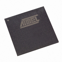
AT94S40AL-25DGC Atmel, AT94S40AL-25DGC Datasheet - Page 12

AT94S40AL-25DGC
Manufacturer Part Number
AT94S40AL-25DGC
Description
IC FPSLIC 40K GATE 25MHZ 256BGA
Manufacturer
Atmel
Series
FPSLIC®r
Datasheet
1.AT94S10AL-25DGC.pdf
(32 pages)
Specifications of AT94S40AL-25DGC
Core Type
8-bit AVR
Speed
16MHz
Interface
I²C, UART
Program Sram Bytes
20K-32K
Fpga Sram
18kb
Eeprom Size
1M x 8
Data Sram Bytes
4K ~ 16K
Fpga Core Cells
2304
Fpga Gates
40K
Fpga Registers
2862
Voltage - Supply
3 V ~ 3.6 V
Mounting Type
Surface Mount
Operating Temperature
0°C ~ 70°C
Package / Case
256-CABGA
Lead Free Status / RoHS Status
Contains lead / RoHS non-compliant
Available stocks
Company
Part Number
Manufacturer
Quantity
Price
4.9.5.3
4.9.6
4.9.7
4.9.8
4.9.8.1
4.9.9
12
AT94S Secure Family
Programmer Functions
Reading Manufacturer’s and Device Codes
Programming the Device
Verifying the Device
Sequential Read
Important Note on AT94S Series Configurators Programming
Sequential Reads follow either a Current Address Read or a Random Address Read. After the
programmer receives a Data Byte, it may respond with an Acknowledge Bit. As long as the Con-
figurator receives an Acknowledge Bit, it will continue to increment the Data Byte address and
serially clock out sequential Data Bytes until the memory address limit is reached.
Sequential Read instruction is terminated when the programmer does not respond with an
Acknowledge Bit but instead generates a Stop Condition following the receipt of a Data Byte.
Note:
The following programmer functions are supported while the Configurator is in programming
mode (i.e., when SER_EN is driven Low):
In the order given above, they are performed in the following manner.
On AT17LV010 Configurator, the sequential reading of these bytes are accomplished by per-
forming a Random Read at EEPROM Address 040000H.
The correct codes are:
Note:
All the bytes in a given page must be written. The page access order is not important but it is
suggested that the Configurator be written sequentially from address 0. Writing is accomplished
by using the cSDA and cSCK pins.
The first byte of data will not be cached for read back during FPGA Configuration (i.e., when
SER_EN is driven High) until the Configurator is power-cycled.
All bytes in the Configurator should be read and compared to their intended values. Reading is
done using the cSDA and cSCK pins.
1. Read the Manufacturer’s Code and the Device Code (optional for ISP).
2. Program the device.
3. Verify the device.
Manufacturers Code -Byte 0
Device Code
1. If an ACK is sent by the programmer after the data in the last memory address is sent by the
The Manufacturer’s Code and Device Code are read using the byte ordering specified for Data
Bytes; i.e., LSB first, MSB last.
configurator, the internal address counter will “rollover” to the first byte address of the memory
array and continue to send data as long as an ACK is sent by the programmer.
- Byte 1 F7
1E
AT17LV010
2314E–FPSLI–6/05
(1)
The


