20-101-0356 Rabbit Semiconductor, 20-101-0356 Datasheet - Page 81
20-101-0356
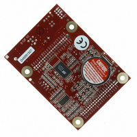
Manufacturer Part Number
20-101-0356
Description
COMPUTER SINGLE-BOARD BL1800
Manufacturer
Rabbit Semiconductor
Datasheet
1.20-101-0356.pdf
(94 pages)
Specifications of 20-101-0356
Module/board Type
Single Board Computer Module
Product
Modules
Data Bus Width
8 bit
Processor Type
Rabbit 2000
Sram
128 KB
Flash
256 KB
Timers
8 bit, 10 bit
Number Of I/os
14
Backup Battery
3 V Lithium Coin Type
Operating Voltage
8 V to 40 V
Power Consumption
1.2 W
Board Size
89 mm x 64 mm x 19 mm
Description/function
Computer Module
For Use With/related Products
BL1800
Lead Free Status / RoHS Status
Lead free / RoHS Compliant
Other names
316-1079


Once the LEDs, resistors, and switches are disconnected as described above, the user has a
Jackrabbit board with connection points conveniently brought out to labeled points at headers
J3 and J7 on the Prototyping Board. Small to medium circuits can be prototyped using point-
to-point wiring with 20 to 30 AWG wire between the prototyping area and the holes at loca-
tions J3 and J7. Note that the pinouts at locations J3 and J7 on the top side of the Prototyping
Board (shown in Figure B-7) are a mirror image of the Jackrabbit board pinouts.
Figure B-7. Jackrabbit I/O Pinout on Prototyping Board (top side)
A user-supplied DE9 connector can be added as shown in Figure B-3. The signals are
brought out to location J5 on the top side of the Prototyping Board.
There are six independent surface-mount 14- to 16-pin SOIC pads and fourteen 3- to 5-pin
SOT23 pads. Each component has every one of its pin pads connected to a hole in the pro-
totyping area. The layout is such that there is another SOIC or SOT23 pad directly on the
other side of the PCB from the SOIC or SOT23 pads. However, each layout location is
routed to its unique set of connection holes. Because the traces are very thin, carefully
determine which set of holes is connected to which surface-mount pad. There are several
standard 0805 passive-component surface-mount pads. These pads are not routed to wir-
ing holes so wire must be soldered directly to the component. In addition, there is a large
generic array of wide traces connected to large holes. This is provided as an additional
area for surface-mount passive components. There is a moderate amount of 0.1” arrayed
through-hole prototyping area (about 137 holes) for mounting through-hole components.
Thus, many circuits requiring special circuitry external to the Jackrabbit can be prototyped
and tested with the Prototyping Board. If additional prototyping space is needed, install
40-pin headers at locations J3 and J7 on the top side of the Prototyping Board to connect
to sockets that you would install at J3 and J7 on the top side of a second Prototyping
Board.
User’s Manual
77
Related parts for 20-101-0356
Image
Part Number
Description
Manufacturer
Datasheet
Request
R

Part Number:
Description:
COMPUTER SGL-BRD BL2500 29.4MHZ
Manufacturer:
Rabbit Semiconductor
Datasheet:

Part Number:
Description:
COMPUTER SGL-BRD BL2500 29.4MHZ
Manufacturer:
Rabbit Semiconductor
Datasheet:

Part Number:
Description:
DISPLAY GRAPHIC 12KEY PROG OP670
Manufacturer:
Rabbit Semiconductor
Datasheet:
Part Number:
Description:
DISPLAY GRAPHIC 12KEY ETH OP6700
Manufacturer:
Rabbit Semiconductor
Datasheet:

Part Number:
Description:
COMPUTER SINGLE-BOARD BL2030
Manufacturer:
Rabbit Semiconductor
Part Number:
Description:
COMPUTER SGL-BOARD ETH BL2010
Manufacturer:
Rabbit Semiconductor

Part Number:
Description:
MODULE OP6810 W/O ETH/MEM EXPANS
Manufacturer:
Rabbit Semiconductor
Datasheet:
Part Number:
Description:
COMPUTER SINGLE-BOARD BL2020
Manufacturer:
Rabbit Semiconductor
Part Number:
Description:
COMPUTER BL2010 W/FRICTION LOCK
Manufacturer:
Rabbit Semiconductor
Part Number:
Description:
COMPUTER BL2020 W/FRICTION LOCK
Manufacturer:
Rabbit Semiconductor
Part Number:
Description:
COMPUTER SGL-BRD BL2500 44.2MHZ
Manufacturer:
Rabbit Semiconductor
Datasheet:
Part Number:
Description:
COMPUTER SGL-BOARD FULL BL2000
Manufacturer:
Rabbit Semiconductor

Part Number:
Description:
COMPUTER SINGLE-BOARD BL2110
Manufacturer:
Rabbit Semiconductor

Part Number:
Description:
COMPUTER SGL-BRD 29.4MHZ BL2610
Manufacturer:
Rabbit Semiconductor
Datasheet:
Part Number:
Description:
INTERFACE OP6800 512K FLASH&SRAM
Manufacturer:
Rabbit Semiconductor
Datasheet: