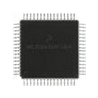
MC68HC908LD60IFU Freescale Semiconductor, MC68HC908LD60IFU Datasheet - Page 151

MC68HC908LD60IFU
Manufacturer Part Number
MC68HC908LD60IFU
Description
Manufacturer
Freescale Semiconductor
Datasheet
1.MC68HC908LD60IFU.pdf
(292 pages)
Specifications of MC68HC908LD60IFU
Cpu Family
HC08
Device Core Size
8b
Frequency (max)
6MHz
Program Memory Type
Flash
Program Memory Size
60KB
Total Internal Ram Size
1KB
# I/os (max)
39
Number Of Timers - General Purpose
2
Operating Supply Voltage (typ)
3.3V
Operating Supply Voltage (max)
3.6V
Operating Supply Voltage (min)
3V
On-chip Adc
6-chx8-bit
Instruction Set Architecture
CISC
Operating Temp Range
0C to 85C
Operating Temperature Classification
Commercial
Mounting
Surface Mount
Pin Count
64
Package Type
PQFP
Lead Free Status / Rohs Status
Compliant
Available stocks
Company
Part Number
Manufacturer
Quantity
Price
- Current page: 151 of 292
- Download datasheet (4Mb)
11.5.4.2 Buffered PWM Signal Generation
MC68HC908LD60
Freescale Semiconductor
NOTE:
—
Rev. 1.1
Use the following methods to synchronize unbuffered changes in the
PWM pulse width on channel x:
In PWM signal generation, do not program the PWM channel to toggle
on output compare. Toggling on output compare prevents reliable 0%
duty cycle generation and removes the ability of the channel to self-
correct in the event of software error or noise. Toggling on output
compare also can cause incorrect PWM signal generation when
changing the PWM pulse width to a new, much larger value.
Channels 0 and 1 can be linked to form a buffered PWM channel whose
output appears on the TCH0 pin. The TIM channel registers of the linked
pair alternately control the pulse width of the output.
Setting the MS0B bit in TIM channel 0 status and control register (TSC0)
links channel 0 and channel 1. The TIM channel 0 registers initially
control the pulse width on the TCH0 pin. Writing to the TIM channel 1
registers enables the TIM channel 1 registers to synchronously control
the pulse width at the beginning of the next PWM period. At each
subsequent overflow, the TIM channel registers (0 or 1) that control the
pulse width are the ones written to last. TSC0 controls and monitors the
buffered PWM function, and TIM channel 1 status and control register
(TSC1) is unused. While the MS0B bit is set, the channel 1 pin, TCH1,
is available as a general-purpose I/O pin.
•
•
When changing to a shorter pulse width, enable channel x output
compare interrupts and write the new value in the output compare
interrupt routine. The output compare interrupt occurs at the end
of the current pulse. The interrupt routine has until the end of the
PWM period to write the new value.
When changing to a longer pulse width, enable channel x TIM
overflow interrupts and write the new value in the TIM overflow
interrupt routine. The TIM overflow interrupt occurs at the end of
the current PWM period. Writing a larger value in an output
compare interrupt routine (at the end of the current pulse) could
cause two output compares to occur in the same PWM period.
Timer Interface Module (TIM)
Timer Interface Module (TIM)
Functional Description
Technical Data
151
Related parts for MC68HC908LD60IFU
Image
Part Number
Description
Manufacturer
Datasheet
Request
R
Part Number:
Description:
Manufacturer:
Freescale Semiconductor, Inc
Datasheet:
Part Number:
Description:
Manufacturer:
Freescale Semiconductor, Inc
Datasheet:
Part Number:
Description:
Manufacturer:
Freescale Semiconductor, Inc
Datasheet:
Part Number:
Description:
Manufacturer:
Freescale Semiconductor, Inc
Datasheet:
Part Number:
Description:
Manufacturer:
Freescale Semiconductor, Inc
Datasheet:
Part Number:
Description:
Manufacturer:
Freescale Semiconductor, Inc
Datasheet:
Part Number:
Description:
Manufacturer:
Freescale Semiconductor, Inc
Datasheet:
Part Number:
Description:
Manufacturer:
Freescale Semiconductor, Inc
Datasheet:
Part Number:
Description:
Manufacturer:
Freescale Semiconductor, Inc
Datasheet:
Part Number:
Description:
Manufacturer:
Freescale Semiconductor, Inc
Datasheet:
Part Number:
Description:
Manufacturer:
Freescale Semiconductor, Inc
Datasheet:
Part Number:
Description:
Manufacturer:
Freescale Semiconductor, Inc
Datasheet:
Part Number:
Description:
Manufacturer:
Freescale Semiconductor, Inc
Datasheet:
Part Number:
Description:
Manufacturer:
Freescale Semiconductor, Inc
Datasheet:
Part Number:
Description:
Manufacturer:
Freescale Semiconductor, Inc
Datasheet:


