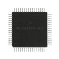
MC68HC908LD60IFU Freescale Semiconductor, MC68HC908LD60IFU Datasheet - Page 63

MC68HC908LD60IFU
Manufacturer Part Number
MC68HC908LD60IFU
Description
Manufacturer
Freescale Semiconductor
Datasheet
1.MC68HC908LD60IFU.pdf
(292 pages)
Specifications of MC68HC908LD60IFU
Cpu Family
HC08
Device Core Size
8b
Frequency (max)
6MHz
Program Memory Type
Flash
Program Memory Size
60KB
Total Internal Ram Size
1KB
# I/os (max)
39
Number Of Timers - General Purpose
2
Operating Supply Voltage (typ)
3.3V
Operating Supply Voltage (max)
3.6V
Operating Supply Voltage (min)
3V
On-chip Adc
6-chx8-bit
Instruction Set Architecture
CISC
Operating Temp Range
0C to 85C
Operating Temperature Classification
Commercial
Mounting
Surface Mount
Pin Count
64
Package Type
PQFP
Lead Free Status / Rohs Status
Compliant
Available stocks
Company
Part Number
Manufacturer
Quantity
Price
- Current page: 63 of 292
- Download datasheet (4Mb)
MC68HC908LD60
Freescale Semiconductor
Algorithm for programming
a row (64 bytes) of FLASH memory
NOTE:
The time between each FLASH address change (step 6 to step 6), or
the time between the last FLASH address programmed
to clearing PGM bit (step 6 to step 9)
must not exceed the maximum programming
time, t
This row program algorithm assumes the row/s
to be programmed are initially erased.
PROG
—
max.
Rev. 1.1
6
For 47,616 bytes array
Figure 4-5. FLASH Programming Flowchart
Write data to the FLASH address
to be programmed
1
2
3
4
5
7
FLASH Memory
Write any data to any FLASH address
within the row address range desired
Wait for a time, t
Wait for a time, t
Wait for a time, t
Set HVEN bit
programming
Set PGM bit
Completed
this row?
N
prog
nvs
pgs
For 13k-bytes array
9
10
11
12
Write even location byte to 13k-byte
FLASH Even Byte Write Buffer at $0066.
Write odd location byte to the odd
FLASH adress to be programmed.
Y
End of Programming
Wait for a time, t
Wait for a time, t
Clear HVEN bit
Clear PGM bit
FLASH Block Protection
nvh
rcv
FLASH Memory
Technical Data
63
Related parts for MC68HC908LD60IFU
Image
Part Number
Description
Manufacturer
Datasheet
Request
R
Part Number:
Description:
Manufacturer:
Freescale Semiconductor, Inc
Datasheet:
Part Number:
Description:
Manufacturer:
Freescale Semiconductor, Inc
Datasheet:
Part Number:
Description:
Manufacturer:
Freescale Semiconductor, Inc
Datasheet:
Part Number:
Description:
Manufacturer:
Freescale Semiconductor, Inc
Datasheet:
Part Number:
Description:
Manufacturer:
Freescale Semiconductor, Inc
Datasheet:
Part Number:
Description:
Manufacturer:
Freescale Semiconductor, Inc
Datasheet:
Part Number:
Description:
Manufacturer:
Freescale Semiconductor, Inc
Datasheet:
Part Number:
Description:
Manufacturer:
Freescale Semiconductor, Inc
Datasheet:
Part Number:
Description:
Manufacturer:
Freescale Semiconductor, Inc
Datasheet:
Part Number:
Description:
Manufacturer:
Freescale Semiconductor, Inc
Datasheet:
Part Number:
Description:
Manufacturer:
Freescale Semiconductor, Inc
Datasheet:
Part Number:
Description:
Manufacturer:
Freescale Semiconductor, Inc
Datasheet:
Part Number:
Description:
Manufacturer:
Freescale Semiconductor, Inc
Datasheet:
Part Number:
Description:
Manufacturer:
Freescale Semiconductor, Inc
Datasheet:
Part Number:
Description:
Manufacturer:
Freescale Semiconductor, Inc
Datasheet:


