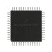
MC68HC908LD60IFU Freescale Semiconductor, MC68HC908LD60IFU Datasheet - Page 282

MC68HC908LD60IFU
Manufacturer Part Number
MC68HC908LD60IFU
Description
Manufacturer
Freescale Semiconductor
Datasheet
1.MC68HC908LD60IFU.pdf
(292 pages)
Specifications of MC68HC908LD60IFU
Cpu Family
HC08
Device Core Size
8b
Frequency (max)
6MHz
Program Memory Type
Flash
Program Memory Size
60KB
Total Internal Ram Size
1KB
# I/os (max)
39
Number Of Timers - General Purpose
2
Operating Supply Voltage (typ)
3.3V
Operating Supply Voltage (max)
3.6V
Operating Supply Voltage (min)
3V
On-chip Adc
6-chx8-bit
Instruction Set Architecture
CISC
Operating Temp Range
0C to 85C
Operating Temperature Classification
Commercial
Mounting
Surface Mount
Pin Count
64
Package Type
PQFP
Lead Free Status / Rohs Status
Compliant
Available stocks
Company
Part Number
Manufacturer
Quantity
Price
- Current page: 282 of 292
- Download datasheet (4Mb)
Electrical Specifications
22.6 DC Electrical Characteristics
Technical Data
282
Notes:
Output high voltage (I
Output low voltage (I
Input high voltage
For +5V rated pins
Input low voltage
For +5V rated pins
V
I/O ports Hi-Z leakage current
Input current
Capacitance
POR re-arm voltage
POR rise time ramp rate
Monitor mode entry voltage
Pull-up resistor
Low-voltage inhibit, trip falling voltage
Low-voltage inhibit, trip rising voltage
Low-voltage inhibit reset/recover hysteresis
1. V
4. Wait I
2. Typical values reflect average measurements at midpoint of voltage range, 25 °C only.
3. Run (operating) I
5. STOP I
6. Maximum is highest voltage that POR is guaranteed.
7. If minimum V
DD
All output pins
All output pins
All ports (except PTD4–PTD7), IRQ, RST, OSC1
HSYNC, VSYNC, IICSDA, IICSCL, DDCSDA,
DDCSCL
All ports (except PTD4–PTD7), IRQ, RST, OSC1
HSYNC, VSYNC, IICSDA, IICSCL, DDCSDA,
DDCSCL
Run, PLL off, f
Wait, PLL off, f
Stop
All input pins (except below pins)
HSYNC, VSYNC
Ports (as input or output)
KBI0–KBI7, RST, IRQ
100 pF on all outputs. CL = 20 pF on OSC2. All ports configured as inputs. OSC2 capacitance linearly affects run I
Measured with all modules enabled.
less than 100 pF on all outputs. C
wait I
V
DD
DD
supply current
(5)
= 3.0 to 3.6 Vdc, V
is reached.
DD
DD
DD
.
measured using external square wave clock source (f
0°C to +85°C
OSC1 grounded, no port pins sourcing current.
DD
OP
OP
Characteristic
is not reached before the internal POR reset is released, RST must be driven low externally until minimum
DD
= 6.0 MHz
= 6.0 MHz
(6)
LOAD
measured using external square wave clock source. All inputs 0.2 V from rail. No dc loads. Less than
LOAD
SS
(7)
= 1.6mA)
= 0 Vdc, T
= –2.0mA)
(3)
Table 22-4. DC Electrical Characteristics
(4)
(1)
L
= 20 pF on OSC2; all ports configured as inputs; OSC2 capacitance linearly affects
A
= T
L
to T
Electrical Specifications
H
, unless otherwise noted.
Symbol
V
V
C
V
R
V
V
V
R
TRIPR
V
TRIPF
V
C
V
I
I
POR
I
OUT
POR
HYS
DD
TST
OH
OL
IN
IL
PU
IH
IN
IL
OSCXCLK
= 24MHz); all inputs 0.2 V from rail; no dc loads;
0.7 × V
V
DD
0.035
V
V
Min
2.4
2.0
30
—
—
—
—
—
—
—
—
—
—
0
SS
SS
+ 1.7
DD
Typ
2.45
100
150
MC68HC908LD60
2.6
45
—
—
—
—
—
—
—
—
—
—
—
—
—
—
9
4
(2)
Freescale Semiconductor
0.2 × V
Max
V
±10
200
100
0.4
5.5
0.8
16
±1
±2
12
60
—
—
—
DD
8
8
6
DD
—
Rev. 1.1
V/ms
Unit
mA
mA
mV
mV
µA
µA
µA
kΩ
pF
V
V
V
V
V
V
V
DD
.
Related parts for MC68HC908LD60IFU
Image
Part Number
Description
Manufacturer
Datasheet
Request
R
Part Number:
Description:
Manufacturer:
Freescale Semiconductor, Inc
Datasheet:
Part Number:
Description:
Manufacturer:
Freescale Semiconductor, Inc
Datasheet:
Part Number:
Description:
Manufacturer:
Freescale Semiconductor, Inc
Datasheet:
Part Number:
Description:
Manufacturer:
Freescale Semiconductor, Inc
Datasheet:
Part Number:
Description:
Manufacturer:
Freescale Semiconductor, Inc
Datasheet:
Part Number:
Description:
Manufacturer:
Freescale Semiconductor, Inc
Datasheet:
Part Number:
Description:
Manufacturer:
Freescale Semiconductor, Inc
Datasheet:
Part Number:
Description:
Manufacturer:
Freescale Semiconductor, Inc
Datasheet:
Part Number:
Description:
Manufacturer:
Freescale Semiconductor, Inc
Datasheet:
Part Number:
Description:
Manufacturer:
Freescale Semiconductor, Inc
Datasheet:
Part Number:
Description:
Manufacturer:
Freescale Semiconductor, Inc
Datasheet:
Part Number:
Description:
Manufacturer:
Freescale Semiconductor, Inc
Datasheet:
Part Number:
Description:
Manufacturer:
Freescale Semiconductor, Inc
Datasheet:
Part Number:
Description:
Manufacturer:
Freescale Semiconductor, Inc
Datasheet:
Part Number:
Description:
Manufacturer:
Freescale Semiconductor, Inc
Datasheet:


