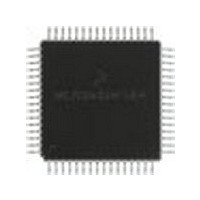
MC68HC908LD60IFU Freescale Semiconductor, MC68HC908LD60IFU Datasheet - Page 62

MC68HC908LD60IFU
Manufacturer Part Number
MC68HC908LD60IFU
Description
Manufacturer
Freescale Semiconductor
Datasheet
1.MC68HC908LD60IFU.pdf
(292 pages)
Specifications of MC68HC908LD60IFU
Cpu Family
HC08
Device Core Size
8b
Frequency (max)
6MHz
Program Memory Type
Flash
Program Memory Size
60KB
Total Internal Ram Size
1KB
# I/os (max)
39
Number Of Timers - General Purpose
2
Operating Supply Voltage (typ)
3.3V
Operating Supply Voltage (max)
3.6V
Operating Supply Voltage (min)
3V
On-chip Adc
6-chx8-bit
Instruction Set Architecture
CISC
Operating Temp Range
0C to 85C
Operating Temperature Classification
Commercial
Mounting
Surface Mount
Pin Count
64
Package Type
PQFP
Lead Free Status / Rohs Status
Compliant
Available stocks
Company
Part Number
Manufacturer
Quantity
Price
- Current page: 62 of 292
- Download datasheet (4Mb)
FLASH Memory
4.8 FLASH Block Protection
Technical Data
62
NOTE:
This program sequence is repeated throughout the memory until all data
is programmed.
Programming and erasing of FLASH locations cannot be performed by
code being executed from the same FLASH array that is being
programmed or erased. While these operations must be performed in
the order shown, other unrelated operations may occur between the
steps. Do not exceed t
Characteristics.
Due to the ability of the on-board charge pump to erase and program the
FLASH memory in the target application, provision is made for protecting
blocks of memory from unintentional erase or program operations due to
system malfunction. This protection is done by use of a FLASH Block
Protect Register for each array (FLBPR and FLBPR1). The block protect
register determines the range of the FLASH memory which is to be
protected. The range of the protected area starts from a location defined
by block protect register and ends at the bottom of the FLASH memory
array ($FFFF and $3FFF). When the memory is protected, the HVEN bit
cannot be set in either ERASE or PROGRAM operations.
10. Wait for time, t
11. Clear the HVEN bit.
12. After time, t
9. Clear the PGM bit.
mode again.
FLASH Memory
rcv
nvh
(min 1µs), the memory can be accessed in read
PROG
(min. 5µs).
maximum. See
22.13 FLASH Memory
MC68HC908LD60
Freescale Semiconductor
—
Rev. 1.1
Related parts for MC68HC908LD60IFU
Image
Part Number
Description
Manufacturer
Datasheet
Request
R
Part Number:
Description:
Manufacturer:
Freescale Semiconductor, Inc
Datasheet:
Part Number:
Description:
Manufacturer:
Freescale Semiconductor, Inc
Datasheet:
Part Number:
Description:
Manufacturer:
Freescale Semiconductor, Inc
Datasheet:
Part Number:
Description:
Manufacturer:
Freescale Semiconductor, Inc
Datasheet:
Part Number:
Description:
Manufacturer:
Freescale Semiconductor, Inc
Datasheet:
Part Number:
Description:
Manufacturer:
Freescale Semiconductor, Inc
Datasheet:
Part Number:
Description:
Manufacturer:
Freescale Semiconductor, Inc
Datasheet:
Part Number:
Description:
Manufacturer:
Freescale Semiconductor, Inc
Datasheet:
Part Number:
Description:
Manufacturer:
Freescale Semiconductor, Inc
Datasheet:
Part Number:
Description:
Manufacturer:
Freescale Semiconductor, Inc
Datasheet:
Part Number:
Description:
Manufacturer:
Freescale Semiconductor, Inc
Datasheet:
Part Number:
Description:
Manufacturer:
Freescale Semiconductor, Inc
Datasheet:
Part Number:
Description:
Manufacturer:
Freescale Semiconductor, Inc
Datasheet:
Part Number:
Description:
Manufacturer:
Freescale Semiconductor, Inc
Datasheet:
Part Number:
Description:
Manufacturer:
Freescale Semiconductor, Inc
Datasheet:


