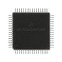
MC68HC908LD60IFU Freescale Semiconductor, MC68HC908LD60IFU Datasheet - Page 179

MC68HC908LD60IFU
Manufacturer Part Number
MC68HC908LD60IFU
Description
Manufacturer
Freescale Semiconductor
Datasheet
1.MC68HC908LD60IFU.pdf
(292 pages)
Specifications of MC68HC908LD60IFU
Cpu Family
HC08
Device Core Size
8b
Frequency (max)
6MHz
Program Memory Type
Flash
Program Memory Size
60KB
Total Internal Ram Size
1KB
# I/os (max)
39
Number Of Timers - General Purpose
2
Operating Supply Voltage (typ)
3.3V
Operating Supply Voltage (max)
3.6V
Operating Supply Voltage (min)
3V
On-chip Adc
6-chx8-bit
Instruction Set Architecture
CISC
Operating Temp Range
0C to 85C
Operating Temperature Classification
Commercial
Mounting
Surface Mount
Pin Count
64
Package Type
PQFP
Lead Free Status / Rohs Status
Compliant
Available stocks
Company
Part Number
Manufacturer
Quantity
Price
- Current page: 179 of 292
- Download datasheet (4Mb)
13.8.2 ADC Data Register
13.8.3 ADC Input Clock Register
MC68HC908LD60
Freescale Semiconductor
—
Rev. 1.1
Address:
Address:
One 8-bit result register, ADC data register (ADR), is provided. This
register is updated each time an ADC conversion completes.
The ADC input clock register (ADICLK) selects the clock frequency for
the ADC.
ADIV[2:0] — ADC Clock Prescaler Bits
Reset:
Reset:
Read:
Read:
Write:
Write:
ADIV[2:0] form a 3-bit field which selects the divide ratio used by the
ADC to generate the internal ADC clock.
available clock configurations. The ADC clock should be set to
approximately 1MHz.
$003C
$003D
ADIV2
Bit 7
AD7
Bit 7
Figure 13-5. ADC Input Clock Register (ADICLK)
Analog-to-Digital Converter (ADC)
0
Figure 13-4. ADC Data Register (ADR)
= Unimplemented
= Unimplemented
ADIV1
AD6
6
6
0
ADIV0
AD5
5
5
0
Indeterminate after Reset
AD4
4
4
0
0
AD3
3
3
0
0
Analog-to-Digital Converter (ADC)
Table 13-2
AD2
2
2
0
0
shows the
AD1
1
1
0
0
Technical Data
I/O Registers
Bit 0
Bit 0
AD0
0
0
179
Related parts for MC68HC908LD60IFU
Image
Part Number
Description
Manufacturer
Datasheet
Request
R
Part Number:
Description:
Manufacturer:
Freescale Semiconductor, Inc
Datasheet:
Part Number:
Description:
Manufacturer:
Freescale Semiconductor, Inc
Datasheet:
Part Number:
Description:
Manufacturer:
Freescale Semiconductor, Inc
Datasheet:
Part Number:
Description:
Manufacturer:
Freescale Semiconductor, Inc
Datasheet:
Part Number:
Description:
Manufacturer:
Freescale Semiconductor, Inc
Datasheet:
Part Number:
Description:
Manufacturer:
Freescale Semiconductor, Inc
Datasheet:
Part Number:
Description:
Manufacturer:
Freescale Semiconductor, Inc
Datasheet:
Part Number:
Description:
Manufacturer:
Freescale Semiconductor, Inc
Datasheet:
Part Number:
Description:
Manufacturer:
Freescale Semiconductor, Inc
Datasheet:
Part Number:
Description:
Manufacturer:
Freescale Semiconductor, Inc
Datasheet:
Part Number:
Description:
Manufacturer:
Freescale Semiconductor, Inc
Datasheet:
Part Number:
Description:
Manufacturer:
Freescale Semiconductor, Inc
Datasheet:
Part Number:
Description:
Manufacturer:
Freescale Semiconductor, Inc
Datasheet:
Part Number:
Description:
Manufacturer:
Freescale Semiconductor, Inc
Datasheet:
Part Number:
Description:
Manufacturer:
Freescale Semiconductor, Inc
Datasheet:


