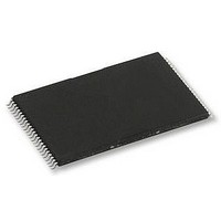
H27UAG8T2ATR-BC HYNIX SEMICONDUCTOR, H27UAG8T2ATR-BC Datasheet - Page 49

H27UAG8T2ATR-BC
Manufacturer Part Number
H27UAG8T2ATR-BC
Description
58T1891
Manufacturer
HYNIX SEMICONDUCTOR
Datasheet
1.H27UAG8T2ATR-BC.pdf
(61 pages)
Specifications of H27UAG8T2ATR-BC
Memory Type
Flash - NAND
Memory Size
16Gbit
Memory Configuration
2048M X 8
Supply Voltage Range
2.7V To 3.6V
Memory Case Style
TSOP
No. Of Pins
48
Operating Temperature Range
0°C To +70°C
Rohs Compliant
Yes
Available stocks
Company
Part Number
Manufacturer
Quantity
Price
Company:
Part Number:
H27UAG8T2ATR-BC
Manufacturer:
HYNIX
Quantity:
2 526
Company:
Part Number:
H27UAG8T2ATR-BC
Manufacturer:
SIEMENS
Quantity:
390
Company:
Part Number:
H27UAG8T2ATR-BC
Manufacturer:
HYNIX
Quantity:
4 000
Part Number:
H27UAG8T2ATR-BC
Manufacturer:
HYNIX/海力士
Quantity:
20 000
Rev 1.0 / Aug. 2010
4.13. Block Erase
The Erase operation is done on a block basis. Block address loading is accomplished in two cycles initiated by an Erase
Setup command (60h). Only address A22 to A31 is valid while A14 to A21 is ignored. The Erase Confirm command
(D0h) following the block address loading initiates the internal erasing process. This two-step sequence of setup fol-
lowed by execution command ensures that memory contents are not accidentally erased due to external noise condi-
tions.
At the rising edge of WE# after the erase confirm command input, the internal write controller handles erase and
erase verify.
Once the erase process starts, the Read Status Register command may be entered to read the status register. The sys-
■ Figure 47. Multi plane Copyback program
R/B#
R/B#
R/B#
I/Ox
I/Ox
I/Ox
R/B#
R/B#
I/Ox
I/Ox
D
A
B
C
00h
85h
81h
60h
00h
Page address : Page M
Plane address : Fixed “Low”
Block address : Block J
Column address : Fixed “Low”
Page address : Page M
Plane address : Fixed “Low”
Block address : Block J
Column address : Valid
Page address : Page N
Plane address : Fixed “Low”
Block address : Block P
Column address : Fixed “Low”
Page address : Page M
Plane address : Fixed “High”
Block address : Block K
Column address : Valid
Page address : Page N
Plane address : Fixed “High”
Block address : Block Q
Address
(5 Cycle)
Address
(5 Cycle)
Address
(5 Cycle)
Address
(3 Cycle)
Address
(5 Cycle)
Data
Data
05h
60h
05h
Page address : Page M
Plane address : Fixed “High”
Block address : Block K
85h
85h
Address
(2 Cycle)
Address
(3 Cycle)
Column address 1,2 : Valid
Column address 1,2 : Valid
Address
(2 Cycle)
Column address 1,2 : Valid
Address
(2 Cycle)
Column address 1,2 : Valid
Address
(2 Cycle)
E0h
35h
E0h
Data
Data
16Gb (2048M x 8bit) NAND Flash
11h
10h
t
R
Data output
Data output
H27UAG8T2B Series
t
DBSY
t
PROG
Release
B
C
D
A
49


