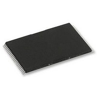
H27UAG8T2ATR-BC HYNIX SEMICONDUCTOR, H27UAG8T2ATR-BC Datasheet - Page 7

H27UAG8T2ATR-BC
Manufacturer Part Number
H27UAG8T2ATR-BC
Description
58T1891
Manufacturer
HYNIX SEMICONDUCTOR
Datasheet
1.H27UAG8T2ATR-BC.pdf
(61 pages)
Specifications of H27UAG8T2ATR-BC
Memory Type
Flash - NAND
Memory Size
16Gbit
Memory Configuration
2048M X 8
Supply Voltage Range
2.7V To 3.6V
Memory Case Style
TSOP
No. Of Pins
48
Operating Temperature Range
0°C To +70°C
Rohs Compliant
Yes
Available stocks
Company
Part Number
Manufacturer
Quantity
Price
Company:
Part Number:
H27UAG8T2ATR-BC
Manufacturer:
HYNIX
Quantity:
2 526
Company:
Part Number:
H27UAG8T2ATR-BC
Manufacturer:
SIEMENS
Quantity:
390
Company:
Part Number:
H27UAG8T2ATR-BC
Manufacturer:
HYNIX
Quantity:
4 000
Part Number:
H27UAG8T2ATR-BC
Manufacturer:
HYNIX/海力士
Quantity:
20 000
Rev 1.0 / Aug. 2010
1.3. PIN DESCRIPTION
I/O0-I/
Name
R/B#
WE#
WP#
CE#
RE#
Pin
CLE
ALE
Vcc
Vss
O7
NC
GROUND
DATA INPUTS/OUTPUTS
The I/O pins are used to COMMAND LATCH cycle, ADDRESS INPUT cycle, and DATA in-out cycles during
read / write operations. The I/O pins float to High-Z when the device is deselected or the outputs are
disabled.
COMMAND LATCH ENABLE
This input activates the latching of the I/O inputs inside the Command Register on the Rising edge of
Write Enable (WE#).
ADDRESS LATCH ENABLE
This input activates the latching of the I/O inputs inside the Address Register on the Rising edge of
Write Enable (WE#).
CHIP ENABLE
This input controls the selection of the device. When the device is busy, CE# low does not deselect the
memory. The device goes into Stand-by mode when CE# goes High during 10us in Ready state. The
CE# signal is ignored when device is in Busy state, and will not enter Standby mode even if the CE#
goes high.
WRITE ENABLE
This input acts as clock to latch Command, Address and Data. The I/O inputs are latched on the rise
edge of WE#.
READ ENABLE
The RE# input is the serial data-out control, and when active drives the data onto the I/O bus. Data is
valid tREA after the falling edge of RE# which also increments the internal column address counter by
one.
WRITE PROTECT
The WP# pin, when Low, provides a hardware protection against undesired write operations. Hardware
Write Protection is activated when the Write Protect pin is low. In this condition modify operation do not
start and the content of the memory is not altered. Write Protect pin is not latched by Write Enable to
ensure the protection even during the power up phases.
READY / BUSY
The Ready/Busy output is an Open Drain pin that signals the state of the memory.
SUPPLY VOLTAGE
The VCC supplies the power for all the operations. (Read, Write, and Erase).
NO CONNECTED
I/O7~I/O0
R/B#
WE#
WP#
CE#
RE#
VCC
CLE
ALE
VSS
NC
Description
Command Latch Enable
Address Latch Enable
Data Input / Outputs
No Connection
Power Supply
Ready / Busy
Write Protect
16Gb (2048M x 8bit) NAND Flash
Write Enable
Read Enable
Chip Enable
Ground
H27UAG8T2B Series
Release
7


