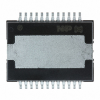
TDA1566TH/N1C,118 NXP Semiconductors, TDA1566TH/N1C,118 Datasheet - Page 15

TDA1566TH/N1C,118
Manufacturer Part Number
TDA1566TH/N1C,118
Description
IC AMP AUDIO PWR 150W AB 24HSOP
Manufacturer
NXP Semiconductors
Type
Class ABr
Datasheet
1.TDA1566THN1C118.pdf
(46 pages)
Specifications of TDA1566TH/N1C,118
Output Type
1-Channel (Mono) or 2-Channel (Stereo)
Package / Case
24-HSOP
Max Output Power X Channels @ Load
150W x 1 @ 1 Ohm; 75W x 2 @ 2 Ohm
Voltage - Supply
6.5 V ~ 18 V
Features
Depop, I²C, Mute, Short-Circuit and Thermal Protection, Standby
Mounting Type
Surface Mount
Product
Class-AB
Output Power
92 W
Available Set Gain
26 dB
Common Mode Rejection Ratio (min)
60 dB
Thd Plus Noise
0.2 %
Operating Supply Voltage
14.4 V
Maximum Power Dissipation
80000 mW
Maximum Operating Temperature
+ 85 C
Mounting Style
SMD/SMT
Audio Load Resistance
4 Ohms
Input Signal Type
Differential
Minimum Operating Temperature
- 40 C
Output Signal Type
Differential
Supply Type
Single
Supply Voltage (max)
18 V
Operational Class
Class-AB
Audio Amplifier Output Configuration
2-Channel Stereo
Audio Amplifier Function
Speaker
Single Supply Voltage (typ)
14.4V
Dual Supply Voltage (typ)
Not RequiredV
Power Supply Requirement
Single
Power Dissipation
80W
Rail/rail I/o Type
No
Single Supply Voltage (max)
18V
Dual Supply Voltage (min)
Not RequiredV
Dual Supply Voltage (max)
Not RequiredV
Operating Temp Range
-40C to 85C
Operating Temperature Classification
Industrial
Mounting
Surface Mount
Pin Count
24
Package Type
HSOP
Lead Free Status / RoHS Status
Lead free / RoHS Compliant
Lead Free Status / RoHS Status
Lead free / RoHS Compliant, Lead free / RoHS Compliant
Other names
935284624118
TDA1566TH/N1C-T
TDA1566TH/N1C-T
TDA1566TH/N1C-T
TDA1566TH/N1C-T
NXP Semiconductors
TDA1566_2
Product data sheet
6.4.1 I
6.4 I
Table 16.
[1]
Table 17.
[1]
ADS1
open
33 k to GND open
ADS1
open
33 k to GND
2
2
Fig 10. Offset detection in I
C-bus address with hardware address select
C-bus operation
0 = write to TDA1566TH; 1 = read from TDA1566TH.
0 = write to TDA1566J; 1 = read from TDA1566J.
threshold
threshold
offset
offset
DB1[D2] read
DB1[D2] =
DB1[D2] read
DB1[D2] =
I
I
2
2
C-bus address table TH version
C-bus address table J version
ADS2
open
GND
GND
A6
1
1
1
1
I
2
C-bus mode only
0
1
Rev. 02 — 20 August 2007
A6
1
1
1
1
V
V
A5
1
1
o
o
= V
= V
0 => 1
1
2
C-bus mode and in non-I
I
OUT+
OUT+
2
C-bus controlled dual channel/single channel amplifier
A5
1
1
1
1
A4
0
0
V
V
OUT
OUT
time
time
A4
0
0
0
0
A3
1
1
threshold
threshold
A3
1
1
1
1
offset
offset
DIAG
DIAG
2
A2
0
0
C-bus mode
TH version only: Non-I
TH/J version:
A2
0
0
0
0
A1
0
1
A1
0
0
1
1
fault selected on DIAG
I
V
V
2
C-bus mode with offset
o
o
= V
= V
TDA1566
2
A0
1
1
© NXP B.V. 2007. All rights reserved.
C-bus mode
OUT+
OUT+
A0
0
1
0
1
001aad013
V
V
OUT
OUT
R/W
1/0
1/0
1/0
1/0
R/W
1/0
1/0
time
time
time
time
15 of 46
[1]
[1]


