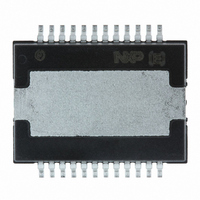
TDA1566TH/N1C,118 NXP Semiconductors, TDA1566TH/N1C,118 Datasheet - Page 27

TDA1566TH/N1C,118
Manufacturer Part Number
TDA1566TH/N1C,118
Description
IC AMP AUDIO PWR 150W AB 24HSOP
Manufacturer
NXP Semiconductors
Type
Class ABr
Datasheet
1.TDA1566THN1C118.pdf
(46 pages)
Specifications of TDA1566TH/N1C,118
Output Type
1-Channel (Mono) or 2-Channel (Stereo)
Package / Case
24-HSOP
Max Output Power X Channels @ Load
150W x 1 @ 1 Ohm; 75W x 2 @ 2 Ohm
Voltage - Supply
6.5 V ~ 18 V
Features
Depop, I²C, Mute, Short-Circuit and Thermal Protection, Standby
Mounting Type
Surface Mount
Product
Class-AB
Output Power
92 W
Available Set Gain
26 dB
Common Mode Rejection Ratio (min)
60 dB
Thd Plus Noise
0.2 %
Operating Supply Voltage
14.4 V
Maximum Power Dissipation
80000 mW
Maximum Operating Temperature
+ 85 C
Mounting Style
SMD/SMT
Audio Load Resistance
4 Ohms
Input Signal Type
Differential
Minimum Operating Temperature
- 40 C
Output Signal Type
Differential
Supply Type
Single
Supply Voltage (max)
18 V
Operational Class
Class-AB
Audio Amplifier Output Configuration
2-Channel Stereo
Audio Amplifier Function
Speaker
Single Supply Voltage (typ)
14.4V
Dual Supply Voltage (typ)
Not RequiredV
Power Supply Requirement
Single
Power Dissipation
80W
Rail/rail I/o Type
No
Single Supply Voltage (max)
18V
Dual Supply Voltage (min)
Not RequiredV
Dual Supply Voltage (max)
Not RequiredV
Operating Temp Range
-40C to 85C
Operating Temperature Classification
Industrial
Mounting
Surface Mount
Pin Count
24
Package Type
HSOP
Lead Free Status / RoHS Status
Lead free / RoHS Compliant
Lead Free Status / RoHS Status
Lead free / RoHS Compliant, Lead free / RoHS Compliant
Other names
935284624118
TDA1566TH/N1C-T
TDA1566TH/N1C-T
TDA1566TH/N1C-T
TDA1566TH/N1C-T
NXP Semiconductors
Table 23.
Refer to test circuit (see
otherwise specified.
[1]
[2]
[3]
[4]
[5]
[6]
[7]
[8]
[9]
[10] R
[11] Power bandwidth can be limited by the 3 dB cut-off frequency, see
TDA1566_2
Product data sheet
Symbol
SVRR
CMRR
V
V
G
G
Z
B
cs
i(sym)
mute
cm(max)(rms)
n(o)(RMS)
p
v(amp)
v(ld)
Operation above 16 V with a 2
restart after 8 ms resulting in an ‘audio hole’.
If the EN pin is connected with V
If the EN pin is left unconnected the amplifier will be switched off.
The mute release is initiated when the SVR voltage increases above 3.5 V typical. Mute release is defined as the moment when the
output signal has reached 10 % of the expected amplitude.
Mute release is defined as the moment when the output signal has reached 10 % of the expected amplitude (G
defined as the moment when the output signal has reached 90 % of the expected amplitude (G
Standard I
maximum LOW level is defined with V
If the 1
Clip detect is not operational for V
If an open load is detected the amplifier is switched in line driver mode.
----------------------------- -
2
s
is the total differential source resistance. 3 dB cut-off frequency is given as
R
1
i
Characteristics
pin is connected with V
2
C
C-bus spec: maximum LOW level = 0.3
i
Parameter
channel separation
supply voltage
rejection ratio
common-mode
rejection ratio
maximum
common-mode
voltage (RMS value)
RMS noise output
voltage
voltage gain amplifier
mode
voltage gain line driver
mode
symmetrical input
impedance
mute attenuation
power bandwidth
=
----------------------------------------------------------------- -
2
Figure
22 k
…continued
22); V
1
470 nF
P
P
or 1
P
a series resistance of 10 k is necessary for load dump robustness.
a series resistance of 10 k is necessary for load dump robustness.
< 10 V.
P
DD
= 14.4 V; R
mode with reactive load can trigger the amplifier protection. The amplifier switches off and will
Conditions
f = 1 kHz to 10 kHz; R
f = 100 Hz to 10 kHz;
R
amplifier mode;
V
3 kHz; R
f = 1 kHz; V
amplifier mode
f = 1 kHz; V
line driver mode
line driver mode; filter 20 Hz to
22 kHz; R
amplifier mode; filter 20 Hz to
22 kHz; R
mute mode; filter 20 Hz to
22 kHz; R
(V
(V
(V
(V
C = 470 nF
f = 1 kHz; V
= 5 V and the minimum HIGH level with V
1 dB; C = 2.2 F
0.8
cm
s
OUT1+
IN1+
OUT1+
IN1+
= 2 k ; V
= 0.3 V (p-p); f = 1 kHz to
=
19 Hz
V
V
s
Rev. 02 — 20 August 2007
L
s
s
s
IN1
IN1
= 2 k
V
V
V
= 4 ; 40 C < T
= 2 k
= 2 k
= 2 k
i
i
OUT
OUT1
i
DD
ripple
= 0.5 V (RMS);
= 1.6 V (RMS);
= 1 V (RMS)
)
)
, minimum HIGH level = 0.7
assuming worst case low input resistance and 20 % spread in C
I
) /
) /
= 2 V (p-p)
2
C-bus controlled dual channel/single channel amplifier
s
= 2 k
Table note
amb
< +85 C and 40 C < T
[10]
[11]
10.
DD
Min
42
45
60
-
-
-
-
-
25
15
44
-
-
= 3.3 V.
V
DD
. To comply with 5 V and 3.3 V logic the
v
V
Typ
55
70
70
-
-
20
50
20
26
16
60
80
20 to
20000
i
).
j
< +150 C; unless
v
TDA1566
Max
-
-
-
1
0.6
50
70
50
27
17
-
-
-
© NXP B.V. 2007. All rights reserved.
V
i
). Full gain is
i
.
Unit
dB
dB
dB
V
V
dB
dB
k
dB
Hz
27 of 46
V
V
V


