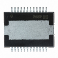
TDA1566TH/N1C,118 NXP Semiconductors, TDA1566TH/N1C,118 Datasheet - Page 18

TDA1566TH/N1C,118
Manufacturer Part Number
TDA1566TH/N1C,118
Description
IC AMP AUDIO PWR 150W AB 24HSOP
Manufacturer
NXP Semiconductors
Type
Class ABr
Datasheet
1.TDA1566THN1C118.pdf
(46 pages)
Specifications of TDA1566TH/N1C,118
Output Type
1-Channel (Mono) or 2-Channel (Stereo)
Package / Case
24-HSOP
Max Output Power X Channels @ Load
150W x 1 @ 1 Ohm; 75W x 2 @ 2 Ohm
Voltage - Supply
6.5 V ~ 18 V
Features
Depop, I²C, Mute, Short-Circuit and Thermal Protection, Standby
Mounting Type
Surface Mount
Product
Class-AB
Output Power
92 W
Available Set Gain
26 dB
Common Mode Rejection Ratio (min)
60 dB
Thd Plus Noise
0.2 %
Operating Supply Voltage
14.4 V
Maximum Power Dissipation
80000 mW
Maximum Operating Temperature
+ 85 C
Mounting Style
SMD/SMT
Audio Load Resistance
4 Ohms
Input Signal Type
Differential
Minimum Operating Temperature
- 40 C
Output Signal Type
Differential
Supply Type
Single
Supply Voltage (max)
18 V
Operational Class
Class-AB
Audio Amplifier Output Configuration
2-Channel Stereo
Audio Amplifier Function
Speaker
Single Supply Voltage (typ)
14.4V
Dual Supply Voltage (typ)
Not RequiredV
Power Supply Requirement
Single
Power Dissipation
80W
Rail/rail I/o Type
No
Single Supply Voltage (max)
18V
Dual Supply Voltage (min)
Not RequiredV
Dual Supply Voltage (max)
Not RequiredV
Operating Temp Range
-40C to 85C
Operating Temperature Classification
Industrial
Mounting
Surface Mount
Pin Count
24
Package Type
HSOP
Lead Free Status / RoHS Status
Lead free / RoHS Compliant
Lead Free Status / RoHS Status
Lead free / RoHS Compliant, Lead free / RoHS Compliant
Other names
935284624118
TDA1566TH/N1C-T
TDA1566TH/N1C-T
TDA1566TH/N1C-T
TDA1566TH/N1C-T
NXP Semiconductors
TDA1566_2
Product data sheet
Fig 11. Start-up and shutdown timing in I
V
DIAG
DB3[D7]
DB3[D4]
IB1[D0]
IB2[D0] = 0
EN
SVR
OUTx
P
t
d(mute_off)
1
t
wake
For optimized pop performance it is recommended to keep the amplifier in mute until the
SVR voltage has reached its final level.
When the amplifier is switched off by pulling the EN pin LOW the amplifier is muted (fast
mute) and the capacitor on the SVR pin will be discharged. With an SVR capacitor of
22 F the off current is reached 2 s after the EN pin is switched to zero.
Start-up and shutdown in I
Table 20.
Step
1
2
2
t
Action
TDA1566 is enabled with EN TDA1566 from off to standby
TDA1566 is switched from
standby to operating with
IB1[D0] = 1
dcload
Start-up and shutdown timing in I
t
d(mute-fgain)
2
C-bus mode
3
Rev. 02 — 20 August 2007
2
C-bus mode is shown in
I
2
C-bus controlled dual channel/single channel amplifier
mute
4
slow
Result
DB3[D7] is set and DIAG is pulled LOW to indicate
power-on reset
DIAG is released
DB3[D7] is reset
SVR capacitor is charged, OUTx voltage tracks SVR
voltage
gradual increase of gain; when the SVR voltage increases
above a threshold of 2 V + 2V
full gain
5
6
2
C-bus mode
7
Figure 11
and explained in
BE
8
mute
fast
the amplifiers operate at
9
TDA1566
© NXP B.V. 2007. All rights reserved.
001aad014
Table
10
18 of 46
20.


