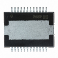
TDA1566TH/N1C,118 NXP Semiconductors, TDA1566TH/N1C,118 Datasheet - Page 42

TDA1566TH/N1C,118
Manufacturer Part Number
TDA1566TH/N1C,118
Description
IC AMP AUDIO PWR 150W AB 24HSOP
Manufacturer
NXP Semiconductors
Type
Class ABr
Datasheet
1.TDA1566THN1C118.pdf
(46 pages)
Specifications of TDA1566TH/N1C,118
Output Type
1-Channel (Mono) or 2-Channel (Stereo)
Package / Case
24-HSOP
Max Output Power X Channels @ Load
150W x 1 @ 1 Ohm; 75W x 2 @ 2 Ohm
Voltage - Supply
6.5 V ~ 18 V
Features
Depop, I²C, Mute, Short-Circuit and Thermal Protection, Standby
Mounting Type
Surface Mount
Product
Class-AB
Output Power
92 W
Available Set Gain
26 dB
Common Mode Rejection Ratio (min)
60 dB
Thd Plus Noise
0.2 %
Operating Supply Voltage
14.4 V
Maximum Power Dissipation
80000 mW
Maximum Operating Temperature
+ 85 C
Mounting Style
SMD/SMT
Audio Load Resistance
4 Ohms
Input Signal Type
Differential
Minimum Operating Temperature
- 40 C
Output Signal Type
Differential
Supply Type
Single
Supply Voltage (max)
18 V
Operational Class
Class-AB
Audio Amplifier Output Configuration
2-Channel Stereo
Audio Amplifier Function
Speaker
Single Supply Voltage (typ)
14.4V
Dual Supply Voltage (typ)
Not RequiredV
Power Supply Requirement
Single
Power Dissipation
80W
Rail/rail I/o Type
No
Single Supply Voltage (max)
18V
Dual Supply Voltage (min)
Not RequiredV
Dual Supply Voltage (max)
Not RequiredV
Operating Temp Range
-40C to 85C
Operating Temperature Classification
Industrial
Mounting
Surface Mount
Pin Count
24
Package Type
HSOP
Lead Free Status / RoHS Status
Lead free / RoHS Compliant
Lead Free Status / RoHS Status
Lead free / RoHS Compliant, Lead free / RoHS Compliant
Other names
935284624118
TDA1566TH/N1C-T
TDA1566TH/N1C-T
TDA1566TH/N1C-T
TDA1566TH/N1C-T
NXP Semiconductors
Table 26.
TDA1566_2
Product data sheet
Mounting
Through-hole mount
Through-hole-surface
mount
Suitability of IC packages for wave, reflow and dipping soldering methods
13.3.2 Wave soldering
13.3.3 Manual soldering
13.4 Package related soldering information
Conventional single wave soldering is not recommended for surface mount devices
(SMDs) or printed-circuit boards with a high component density, as solder bridging and
non-wetting can present major problems.
To overcome these problems the double-wave soldering method was specifically
developed.
If wave soldering is used the following conditions must be observed for optimal results:
During placement and before soldering, the package must be fixed with a droplet of
adhesive. The adhesive can be applied by screen printing, pin transfer or syringe
dispensing. The package can be soldered after the adhesive is cured.
Typical dwell time of the leads in the wave ranges from 3 seconds to 4 seconds at 250 C
or 265 C, depending on solder material applied, SnPb or Pb-free respectively.
A mildly-activated flux will eliminate the need for removal of corrosive residues in most
applications.
Fix the component by first soldering two diagonally-opposite end leads. Use a low voltage
(24 V or less) soldering iron applied to the flat part of the lead. Contact time must be
limited to 10 seconds at up to 300 C.
When using a dedicated tool, all other leads can be soldered in one operation within
2 seconds to 5 seconds between 270 C and 320 C.
Package
CPGA, HCPGA
DBS, DIP, HDIP, RDBS, SDIP, SIL
PMFP
•
•
•
Use a double-wave soldering method comprising a turbulent wave with high upward
pressure followed by a smooth laminar wave.
For packages with leads on two sides and a pitch (e):
– larger than or equal to 1.27 mm, the footprint longitudinal axis is preferred to be
– smaller than 1.27 mm, the footprint longitudinal axis must be parallel to the
The footprint must incorporate solder thieves at the downstream end.
For packages with leads on four sides, the footprint must be placed at a 45 angle to
the transport direction of the printed-circuit board. The footprint must incorporate
solder thieves downstream and at the side corners.
[4]
parallel to the transport direction of the printed-circuit board;
transport direction of the printed-circuit board.
[1]
Rev. 02 — 20 August 2007
I
2
C-bus controlled dual channel/single channel amplifier
Soldering method
Wave
suitable
suitable
not suitable
[3]
Reflow
not suitable
[2]
TDA1566
© NXP B.V. 2007. All rights reserved.
Dipping
suitable
42 of 46


