APMOTOR56F8000E Freescale Semiconductor, APMOTOR56F8000E Datasheet - Page 9
APMOTOR56F8000E
Manufacturer Part Number
APMOTOR56F8000E
Description
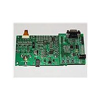
KIT DEMO MOTOR CTRL SYSTEM
Manufacturer
Freescale Semiconductor
Type
Motor / Motion Controllers & Driversr
Datasheets
1.CWH-UTP-ONCE-HE.pdf
(2 pages)
2.APMOTOR56F8000E.pdf
(124 pages)
3.APMOTOR56F8000E.pdf
(2 pages)
Specifications of APMOTOR56F8000E
Accessory Type
Motor Controller
Input Voltage
9 V
Interface Type
RS-232
Product
Power Management Modules
For Use With/related Products
DEMO56F8013, DEMO56F8013-E
Lead Free Status / RoHS Status
Lead free / RoHS Compliant


create a complete, scalable tools solution for easy, fast, and efficient development.
1.4 Architecture Block Diagram
The 56F8014’s architecture is shown in
how the 56800E system buses communicate with internal memories and the IPBus Bridge, as well as
showing the internal connections between each unit of the 56800E core.
and control blocks connected to the IPBus Bridge.
The figures do not show the on-board regulator and power and ground signals. They also do not show the
multiplexing between peripherals or the dedicated GPIOs. Please see
Descriptions
1.5 Synchronize ADC with PWM
ADC conversion can be synchronized with the PWM module via Quad Timer channel 2 and 3 if needed.
Internally, the PWM synch signal — which is generated at every PWM reload —can be connected to the
timer channel 3 input, and the timer channel 2 and channel 3 outputs are connected to the ADC sync inputs.
Timer channel 3 output is connected to SYNC0 and timer channel 2 is connected to SYNC1. The setting
is controlled by the TC3_INP bit in the SIM Control Register; see
SYNC0 is the master ADC sync input, used to trigger both ADCA and ADCB in sequence and parallel
mode. SYNC1 is used to trigger ADCB in parallel independent mode, while SYNC0 is used to trigger
ADCA. See MC56F8000RM, the 56F801X Peripheral Reference Manual, for additional information.
1.6 Multiple Frequency PWM Output
When both PWM channels of a complementary pair in software control mode and software control bits
are set to 1, each complementary PWM signal pair — PWM 0 and 1; PWM 2 and 3; and PWM 4 and 5 —
can select a PWM source from one of the following sources. This will enable each PWM pair and PWM2
to output PWM signals at different frequencies.
Freescale Semiconductor
•
•
•
External GPIO input:
— GPIOB2 input can be used to drive PWM 0 and 1
— GPIOB3 input can be used to drive PWM 2
— GPIOB4 input can be used to drive PWM 4 and 5
Quad Timer output:
— Timer0 output can be used to drive PWM 0 and 1
— Timer2 output can be used to drive PWM 2
— Timer3 output can be used to drive PWM 4 and 5
ADC conversion result:
— Signal of over/under limit of ADC sample 0 can be used to drive PWM 0 and 1
— Signal of over/under limit of ADC sample 1 can be used to drive PWM 2
to see which signals are multiplexed with those of other peripherals.
56F8014 Technical Data, Rev. 11
Figure
1-1,
Figure 1-3
Figure
details how the device’s I/O pins are muxed.
1-2, and
Section
Figure
Figure 1-2
6.3.1.
Part 2 Signal/Connection
1-3.
Figure 1-1
shows the peripherals
Architecture Block Diagram
illustrates
9
Related parts for APMOTOR56F8000E
Image
Part Number
Description
Manufacturer
Datasheet
Request
R

Part Number:
Description:
Manufacturer:
Freescale Semiconductor, Inc
Datasheet:
Part Number:
Description:
Manufacturer:
Freescale Semiconductor, Inc
Datasheet:
Part Number:
Description:
Manufacturer:
Freescale Semiconductor, Inc
Datasheet:
Part Number:
Description:
Manufacturer:
Freescale Semiconductor, Inc
Datasheet:
Part Number:
Description:
Manufacturer:
Freescale Semiconductor, Inc
Datasheet:
Part Number:
Description:
Manufacturer:
Freescale Semiconductor, Inc
Datasheet:
Part Number:
Description:
Manufacturer:
Freescale Semiconductor, Inc
Datasheet:
Part Number:
Description:
Manufacturer:
Freescale Semiconductor, Inc
Datasheet:
Part Number:
Description:
Manufacturer:
Freescale Semiconductor, Inc
Datasheet:
Part Number:
Description:
Manufacturer:
Freescale Semiconductor, Inc
Datasheet:
Part Number:
Description:
Manufacturer:
Freescale Semiconductor, Inc
Datasheet:
Part Number:
Description:
Manufacturer:
Freescale Semiconductor, Inc
Datasheet:
Part Number:
Description:
Manufacturer:
Freescale Semiconductor, Inc
Datasheet:
Part Number:
Description:
Manufacturer:
Freescale Semiconductor, Inc
Datasheet:
Part Number:
Description:
Manufacturer:
Freescale Semiconductor, Inc
Datasheet: