EVAL-ADV7180LFEBZ Analog Devices Inc, EVAL-ADV7180LFEBZ Datasheet - Page 13
EVAL-ADV7180LFEBZ
Manufacturer Part Number
EVAL-ADV7180LFEBZ
Description
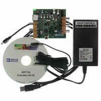
BOARD EVAL FOR ADV7180 LFCSP
Manufacturer
Analog Devices Inc
Specifications of EVAL-ADV7180LFEBZ
Main Purpose
Video, SDTV Video Decoder - NTSC, PAL, SECAM
Embedded
No
Utilized Ic / Part
ADV7180
Primary Attributes
CVBS (Composite), Y/C (S-video), and YPrPb (Component) Inputs
Secondary Attributes
8-bit ITU-R BT.656 YCrCb 4:2:2 Output
Lead Free Status / RoHS Status
Lead free / RoHS Compliant
Available stocks
Company
Part Number
Manufacturer
Quantity
Price
Company:

Part Number:
EVAL-ADV7180LFEBZ
Manufacturer:
Analog Devices Inc
Quantity:
135


40-LEAD LFCSP
Table 10. 40-Lead LFCSP Pin Function Descriptions
Pin No.
1, 4
2
3, 15, 35, 40
5 to 10, 16, 17
11
12
13
14, 36
18
19
20
21, 24, 28
22
23, 29, 30
25
26
27
31
32
33
34
37
38
39
Mnemonic
DVDDIO
SFL
DGND
P7 to P2, P1, P0
LLC
XTAL1
XTAL
DVDD
PWRDWN
ELPF
PVDD
AGND
TEST_0
A
VREFP
VREFN
AVDD
RESET
ALSB
SDATA
SCLK
VS/FIELD
INTRQ
HS
EPAD (EP)
IN
1 to A
IN
3
Type
P
O
G
O
O
O
I
P
I
I
P
G
I
I
O
O
P
I
I
I/O
I
O
O
O
Description
Digital I/O Supply Voltage (1.8 V to 3.3 V).
Subcarrier Frequency Lock. This pin contains a serial output stream that can be used to lock the
subcarrier frequency when this decoder is connected to any Analog Devices digital video encoder.
Ground for Digital Supply.
Video Pixel Output Port.
Line-Locked Output Clock for the Output Pixel Data. Nominally 27 MHz but varies up or
down according to video line length.
This pin should be connected to the 28.6363 MHz crystal or not connected if an external 1.8 V,
28.6363 MHz clock oscillator source is used to clock the ADV7180. In crystal mode, the crystal
must be a fundamental crystal.
Input Pin for the 28.6363 MHz Crystal. This pin can be overdriven by an external 1.8 V,
28.6363 MHz clock oscillator source. In crystal mode, the crystal must be a fundamental crystal.
Digital Supply Voltage (1.8 V).
A logic low on this pin places the ADV7180 into power-down mode.
The recommended external loop filter must be connected to this ELPF pin, as shown in Figure 56.
PLL Supply Voltage (1.8 V).
Ground for Analog Supply.
This pin must be tied to DGND.
Analog Video Input Channels.
Internal Voltage Reference Output. See Figure 56 for recommended output circuitry.
Internal Voltage Reference Output. See Figure 56 for recommended output circuitry.
Analog Supply Voltage (1.8 V).
System Reset Input. Active low. A minimum low reset pulse width of 5 ms is required to
reset the ADV7180 circuitry.
This pin selects the I
for a write is 0x40; for ALSB set to Logic 1, the address selected is 0x42.
I
I
Vertical Synchronization Output Signal/Field Synchronization Output Signal.
Interrupt Request Output. Interrupt occurs when certain signals are detected on the input video
(see Table 108).
Horizontal Synchronization Output Signal.
The exposed pad must be connected to GND.
DVDDIO
DVDDIO
NOTES
1. THE EXPOSED PAD MUST BE CONNECTED TO GND.
2
2
C Port Serial Data Input/Output Pin.
C Port Serial Clock Input. The maximum clock rate is 400 kHz.
DGND
SFL
P7
P6
P5
P4
P3
P2
Figure 9. 40-Lead LFCSP Pin Configuration
10
1
2
3
4
5
6
7
8
9
Rev. F | Page 13 of 116
PIN 1
INDICATOR
(Not to Scale)
ADV7180
TOP VIEW
LFCSP
2
C address for the ADV7180. For ALSB set to Logic 0, the address selected
30
29
28
27
26
25
24
23
22
21
A
A
AGND
AVDD
VREFN
VREFP
AGND
A
TEST_0
AGND
IN
IN
IN
3
2
1
ADV7180
Related parts for EVAL-ADV7180LFEBZ
Image
Part Number
Description
Manufacturer
Datasheet
Request
R

Part Number:
Description:
IC, ADJ LDO REG, 1.5V TO 5V 250mA MSOP-8
Manufacturer:
Vishay
Datasheet:

Part Number:
Description:
IC, ADJ LDO REG, 1.5V TO 5V 0.6A 8-TSSOP
Manufacturer:
Vishay
Datasheet:
Part Number:
Description:
IC, ADJ LDO REG, 1.5V TO 5V 250mA MSOP-8
Manufacturer:
Vishay
Datasheet:

Part Number:
Description:
IC ADJ LDO REG 1.5V TO 5V 150mA 5-SOT-23
Manufacturer:
Vishay
Datasheet:

Part Number:
Description:
BOARD EVAL AS1324-AD
Manufacturer:
austriamicrosystems
Datasheet:
Part Number:
Description:
IC, ADJ LDO REG, 1.5V TO 5V 0.6A 8-TSSOP
Manufacturer:
Vishay
Datasheet:

Part Number:
Description:
IC, ADJ LDO REG, 1.5V TO 5V, 0.3A, MSOP8
Manufacturer:
Vishay
Datasheet:
Part Number:
Description:
IC, ADJ LDO REG, 1.5V TO 5V, 0.3A, MSOP8
Manufacturer:
Vishay
Datasheet:
Part Number:
Description:
IC, ADJ LDO REG 1.215V TO 5V 0.3A MSOP-8
Manufacturer:
Vishay
Datasheet:
Part Number:
Description:
IC, ADJ LDO REG 1.215V TO 5V 0.3A MSOP-8
Manufacturer:
Vishay
Datasheet:

Part Number:
Description:
±1.7g Dual-Axis IMEMS Accelerometer Evaluation Board
Manufacturer:
Analog Devices Inc
Datasheet:

Part Number:
Description:
IC MULTIPLIER ANALOG 8-SOIC T/R
Manufacturer:
Analog Devices Inc
Datasheet:

Part Number:
Description:
IC ANALOG MULTIPLIER 8-DIP
Manufacturer:
Analog Devices Inc
Datasheet:
Part Number:
Description:
IC ANALOG MULTIPLIER 8-SOIC
Manufacturer:
Analog Devices Inc
Datasheet:
Part Number:
Description:
IC ANALOG MULTIPLIER 8-DIP
Manufacturer:
Analog Devices Inc
Datasheet: