EVAL-ADV7180LFEBZ Analog Devices Inc, EVAL-ADV7180LFEBZ Datasheet - Page 9
EVAL-ADV7180LFEBZ
Manufacturer Part Number
EVAL-ADV7180LFEBZ
Description
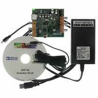
BOARD EVAL FOR ADV7180 LFCSP
Manufacturer
Analog Devices Inc
Specifications of EVAL-ADV7180LFEBZ
Main Purpose
Video, SDTV Video Decoder - NTSC, PAL, SECAM
Embedded
No
Utilized Ic / Part
ADV7180
Primary Attributes
CVBS (Composite), Y/C (S-video), and YPrPb (Component) Inputs
Secondary Attributes
8-bit ITU-R BT.656 YCrCb 4:2:2 Output
Lead Free Status / RoHS Status
Lead free / RoHS Compliant
Available stocks
Company
Part Number
Manufacturer
Quantity
Price
Company:

Part Number:
EVAL-ADV7180LFEBZ
Manufacturer:
Analog Devices Inc
Quantity:
135


TIMING SPECIFICATIONS
Guaranteed by characterization. A
at operating temperature range, unless otherwise noted.
Table 5.
Parameter
SYSTEM CLOCK AND CRYSTAL
I
RESET FEATURE
CLOCK OUTPUTS
DATA AND CONTROL OUTPUTS
Timing Diagrams
2
C PORT
Nominal Frequency
Frequency Stability
SCLK Frequency
SCLK Minimum Pulse Width High
SCLK Minimum Pulse Width Low
Hold Time (Start Condition)
Setup Time (Start Condition)
SDA Setup Time
SCLK and SDA Rise Times
SCLK and SDA Fall Times
Setup Time for Stop Condition
Reset Pulse Width
LLC Mark Space Ratio
Data Output Transitional Time
Data Output Transitional Time
SDATA
SCLK
OUTPUTS P0 TO P15, VS,
VDD
= 1.71 V to 1.89 V, D
OUTPUT LLC
t
3
HS, FIELD,
Symbol
t
t
t
t
t
t
t
t
t
t
t
t
1
2
3
4
5
6
7
8
9
11
12
2
:t
SFL
10
Figure 7. Pixel Port and Control Output Timing
t
6
Test Conditions
Negative clock edge to start of valid data
(t
End of valid data to negative clock edge
(t
ACCESS
HOLD
t
7
VDD
t
1
= t
Rev. F | Page 9 of 116
t
Figure 6. I
= t
5
= 1.65 V to 2.0 V, D
9
10
+ t
− t
12
t
)
9
11
2
C Timing
t
12
)
t
11
t
10
VDDIO
t
= 1.62 V to 3.6 V, P
3
t
4
Min
0.6
1.3
0.6
0.6
100
5
45:55
t
8
Typ
28.6363
0.6
VDD
= 1.65 V to 2.0 V, specified
Max
±50
400
300
300
55:45
3.6
2.4
ADV7180
Unit
MHz
ppm
kHz
μs
μs
μs
μs
ns
ns
ns
μs
ms
% duty cycle
ns
ns
Related parts for EVAL-ADV7180LFEBZ
Image
Part Number
Description
Manufacturer
Datasheet
Request
R

Part Number:
Description:
IC, ADJ LDO REG, 1.5V TO 5V 250mA MSOP-8
Manufacturer:
Vishay
Datasheet:

Part Number:
Description:
IC, ADJ LDO REG, 1.5V TO 5V 0.6A 8-TSSOP
Manufacturer:
Vishay
Datasheet:
Part Number:
Description:
IC, ADJ LDO REG, 1.5V TO 5V 250mA MSOP-8
Manufacturer:
Vishay
Datasheet:

Part Number:
Description:
IC ADJ LDO REG 1.5V TO 5V 150mA 5-SOT-23
Manufacturer:
Vishay
Datasheet:

Part Number:
Description:
BOARD EVAL AS1324-AD
Manufacturer:
austriamicrosystems
Datasheet:
Part Number:
Description:
IC, ADJ LDO REG, 1.5V TO 5V 0.6A 8-TSSOP
Manufacturer:
Vishay
Datasheet:

Part Number:
Description:
IC, ADJ LDO REG, 1.5V TO 5V, 0.3A, MSOP8
Manufacturer:
Vishay
Datasheet:
Part Number:
Description:
IC, ADJ LDO REG, 1.5V TO 5V, 0.3A, MSOP8
Manufacturer:
Vishay
Datasheet:
Part Number:
Description:
IC, ADJ LDO REG 1.215V TO 5V 0.3A MSOP-8
Manufacturer:
Vishay
Datasheet:
Part Number:
Description:
IC, ADJ LDO REG 1.215V TO 5V 0.3A MSOP-8
Manufacturer:
Vishay
Datasheet:

Part Number:
Description:
±1.7g Dual-Axis IMEMS Accelerometer Evaluation Board
Manufacturer:
Analog Devices Inc
Datasheet:

Part Number:
Description:
IC MULTIPLIER ANALOG 8-SOIC T/R
Manufacturer:
Analog Devices Inc
Datasheet:

Part Number:
Description:
IC ANALOG MULTIPLIER 8-DIP
Manufacturer:
Analog Devices Inc
Datasheet:
Part Number:
Description:
IC ANALOG MULTIPLIER 8-SOIC
Manufacturer:
Analog Devices Inc
Datasheet:
Part Number:
Description:
IC ANALOG MULTIPLIER 8-DIP
Manufacturer:
Analog Devices Inc
Datasheet: