EVAL-ADV7180LFEBZ Analog Devices Inc, EVAL-ADV7180LFEBZ Datasheet - Page 50
EVAL-ADV7180LFEBZ
Manufacturer Part Number
EVAL-ADV7180LFEBZ
Description
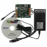
BOARD EVAL FOR ADV7180 LFCSP
Manufacturer
Analog Devices Inc
Specifications of EVAL-ADV7180LFEBZ
Main Purpose
Video, SDTV Video Decoder - NTSC, PAL, SECAM
Embedded
No
Utilized Ic / Part
ADV7180
Primary Attributes
CVBS (Composite), Y/C (S-video), and YPrPb (Component) Inputs
Secondary Attributes
8-bit ITU-R BT.656 YCrCb 4:2:2 Output
Lead Free Status / RoHS Status
Lead free / RoHS Compliant
Available stocks
Company
Part Number
Manufacturer
Quantity
Price
Company:

Part Number:
EVAL-ADV7180LFEBZ
Manufacturer:
Analog Devices Inc
Quantity:
135


ADV7180
Table 66. User Settings for PAL (See Figure 42)
Register
0x31
0x32
0x33
0x34
0x35
0x36
0x37
0xE8
0xE9
0xEA
PVBEGDELO, PAL VSYNC Begin Delay on Odd Field,
Address 0xE8[7]
When PVBEGDELO is 0 (default), there is no delay.
Setting PVBEGDELO to 1 delays VSYNC going high on an odd
field by a line relative to PVBEG.
PVBEGDELE, PAL VSYNC Begin Delay on Even Field,
Address 0xE8[6]
When PVBEGDELE is 0, there is no delay.
Setting PVBEGDELE to 1 (default) delays VSYNC going high
on an even field by a line relative to PVBEG.
PVBEGSIGN, PAL VSYNC Begin Sign, Address 0xE8[5]
Setting PVBEGSIGN to 0 delays the beginning of VSYNC. Set
for user manual programming.
Setting PVBEGSIGN to 1 (default) advances the beginning of
VSYNC (not recommended for user programming).
OUTPUT
OUTPUT
OUTPUT
OUTPUT
OUTPUT
OUTPUT
OUTPUT
OUTPUT
VIDEO
VIDEO
FIELD
FIELD
HS
HS
VS
VS
622
310
Register Name
VS/FIELD Control 1
VS/FIELD Control 2
VS/FIELD Control 3
HS Position Control 1
HS Position Control 2
HS Position Control 3
Polarity
PAL V bit begin
PAL V bit end
PAL F bit toggle
311
623
624
312
Figure 42. PAL Typical VS/FIELD Positions Using the Register Writes Shown in Table 66
625
313
FIELD 1
1
FIELD 2
314
Write
0x1A
0x81
0x84
0x00
0x00
0x7D
0xA1
0x41
0x84
0x06
315
2
PVBEG[4:0] = 0x01
PVBEG[4:0] = 0x01
3
316
Rev. F | Page 50 of 116
317
4
5
318
PVEND[4:0] = 0x04
PVBEG[4:0], PAL VSYNC Begin, Address 0xE8[4:0]
The default value of PVBEG is 00101, indicating the PAL VSYNC
begin position. For all NTSC/PAL VSYNC timing controls, the
V bit in the AV code and the VSYNC signal on the VS pin are
modified.
PVEND[4:0] = 0x04
319
6
NOT VALID FOR USER
PROGRAMMING
7
320
VSYNC BY PVBEG[4:0]
ADVANCE BEGIN OF
ADVANCE BY
PVBEGDELO
ADDITIONAL
321
8
DELAY BY
PFTOG[4:0] = 0x06
0.5 LINE
VSBHO
1 LINE
YES
PFTOG[4:0] = 0x06
1
1
Figure 43. PAL VSYNC Begin
322
9
1
323
10
VSYNC BEGIN
0
0
PVBEGSIGN
ODD FIELD?
11
336
0
0
VSYNC BY PVBEG[4:0]
DELAY BEGIN OF
337
23
ADVANCE BY
PVBEGDELE
ADDITIONAL
DELAY BY
0
0.5 LINE
VSBHE
1 LINE
NO
1
1
24
Related parts for EVAL-ADV7180LFEBZ
Image
Part Number
Description
Manufacturer
Datasheet
Request
R

Part Number:
Description:
IC, ADJ LDO REG, 1.5V TO 5V 250mA MSOP-8
Manufacturer:
Vishay
Datasheet:

Part Number:
Description:
IC, ADJ LDO REG, 1.5V TO 5V 0.6A 8-TSSOP
Manufacturer:
Vishay
Datasheet:
Part Number:
Description:
IC, ADJ LDO REG, 1.5V TO 5V 250mA MSOP-8
Manufacturer:
Vishay
Datasheet:

Part Number:
Description:
IC ADJ LDO REG 1.5V TO 5V 150mA 5-SOT-23
Manufacturer:
Vishay
Datasheet:

Part Number:
Description:
BOARD EVAL AS1324-AD
Manufacturer:
austriamicrosystems
Datasheet:
Part Number:
Description:
IC, ADJ LDO REG, 1.5V TO 5V 0.6A 8-TSSOP
Manufacturer:
Vishay
Datasheet:

Part Number:
Description:
IC, ADJ LDO REG, 1.5V TO 5V, 0.3A, MSOP8
Manufacturer:
Vishay
Datasheet:
Part Number:
Description:
IC, ADJ LDO REG, 1.5V TO 5V, 0.3A, MSOP8
Manufacturer:
Vishay
Datasheet:
Part Number:
Description:
IC, ADJ LDO REG 1.215V TO 5V 0.3A MSOP-8
Manufacturer:
Vishay
Datasheet:
Part Number:
Description:
IC, ADJ LDO REG 1.215V TO 5V 0.3A MSOP-8
Manufacturer:
Vishay
Datasheet:

Part Number:
Description:
±1.7g Dual-Axis IMEMS Accelerometer Evaluation Board
Manufacturer:
Analog Devices Inc
Datasheet:

Part Number:
Description:
IC MULTIPLIER ANALOG 8-SOIC T/R
Manufacturer:
Analog Devices Inc
Datasheet:

Part Number:
Description:
IC ANALOG MULTIPLIER 8-DIP
Manufacturer:
Analog Devices Inc
Datasheet:
Part Number:
Description:
IC ANALOG MULTIPLIER 8-SOIC
Manufacturer:
Analog Devices Inc
Datasheet:
Part Number:
Description:
IC ANALOG MULTIPLIER 8-DIP
Manufacturer:
Analog Devices Inc
Datasheet: