EVAL-ADV7180LFEBZ Analog Devices Inc, EVAL-ADV7180LFEBZ Datasheet - Page 21
EVAL-ADV7180LFEBZ
Manufacturer Part Number
EVAL-ADV7180LFEBZ
Description
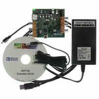
BOARD EVAL FOR ADV7180 LFCSP
Manufacturer
Analog Devices Inc
Specifications of EVAL-ADV7180LFEBZ
Main Purpose
Video, SDTV Video Decoder - NTSC, PAL, SECAM
Embedded
No
Utilized Ic / Part
ADV7180
Primary Attributes
CVBS (Composite), Y/C (S-video), and YPrPb (Component) Inputs
Secondary Attributes
8-bit ITU-R BT.656 YCrCb 4:2:2 Output
Lead Free Status / RoHS Status
Lead free / RoHS Compliant
Available stocks
Company
Part Number
Manufacturer
Quantity
Price
Company:

Part Number:
EVAL-ADV7180LFEBZ
Manufacturer:
Analog Devices Inc
Quantity:
135


GLOBAL CONTROL REGISTERS
Register control bits listed in this section affect the whole chip.
POWER-SAVING MODES
Power-Down
PDBP, Address 0x0F[2]
The digital supply of the ADV7180 can be shut down by using
the PWRDWN pin or via I
0x0F[5]
pin has the higher priority. The default is to give the pin
(
ADV7180 powered down by default at power-up without the
need for an I
When PDBP is 0 (default), the digital supply power is controlled by
the PWRDWN pin (the PWRDWN bit, 0x0F[5], is disregarded).
When PDBP is 1, the PWRDWN bit has priority (the pin is
disregarded).
PWRDWN, Address 0x0F[5]
When PDBP is set to 1, setting the PWRDWN bit switches the
ADV7180 to a chip-wide power-down mode. The power-down
stops the clock from entering the digital section of the chip,
thereby freezing its operation. No I
down. The PWRDWN bit also affects the analog blocks and
switches them into low current modes. The I
unaffected and remains operational in power-down mode.
The ADV7180 leaves the power-down state if the PWRDWN bit is
set to 0 (via I
PDBP must be set to 1 for the PWRDWN bit to power down
the ADV7180.
When PWRDWN is 0 (default), the chip is operational. When
PWRDWN is 1, the ADV7180 is in a chip-wide power-down mode.
RESET CONTROL
Reset, Chip Reset, Address 0x0F[7]
Setting this bit, which is equivalent to controlling the RESET pin
on the ADV7180, issues a full chip reset. All I
to their default/power-up values. Note that some register bits do
not have a reset value specified. They keep their last written value.
Those bits are marked as having a reset value of x in the register
tables (see
the part immediately starts to acquire the incoming video signal.
1
2
PWRDWN ) priority . This allows the user to have the
For 32-lead, I
For 64-lead, 48-lead, and 40-lead only.
section). PDBP controls whether the I
Table 107
2
2
C is the only power-down option.
2
C) or if the ADV7180 is reset using the RESET pin.
C write.
2
and
2
Table 108
2
C (see the
1
2
C bits are lost during power-
). After the reset sequence,
PWRDWN, Address
2
C registers are reset
2
C interface is
2
C control or the
Rev. F | Page 21 of 116
After setting the reset bit (or initiating a reset via the RESET pin),
the part returns to the default for its primary mode of operation.
All I
self-clearing.
Executing a software reset takes approximately 2 ms. However,
it is recommended to wait 5 ms before any further I
performed.
The I
on the ninth clock cycle when chip reset is implemented (see
the MPU Port Description section).
When the reset bit is 0 (default), operation is normal.
When the reset bit is 1, the reset sequence starts.
GLOBAL PIN CONTROL
Three-State Output Drivers
TOD, Address 0x03[6]
This bit allows the user to three-state the output drivers of the
ADV7180.
Upon setting the TOD bit, the P15 to P0 (P7 to P0 for the 48-lead,
40-lead, and 32-lead devices), HS, VS, FIELD (VS/FIELD pin for
the 48-lead, 40-lead, and 32-lead LFCSP), and SFL pins are
three-stated.
The timing pins (HS, VS, FIELD) can be forced active via the
TIM_OE bit. For more information on three-state control, see
the Three-State LLC Driver and the Timing Signals Output
Enable sections.
Individual drive strength controls are provided via the
DR_STR_x bits.
When TOD is 0 (default), the output drivers are enabled.
When TOD is 1, the output drivers are three-stated.
Three-State LLC Driver
TRI_LLC, Address 0x1D[7]
This bit allows the output drivers for the LLC pin of the
ADV7180 to be three-stated. For more information on three-
state control, refer to the Three-State Output Drivers and the
Timing Signals Output Enable sections.
Individual drive strength controls are provided via the
DR_STR_x bits.
When TRI_LLC is 0 (default), the LLC pin drivers work
according to the DR_STR_C[1:0] setting (pin enabled).
When TRI_LLC is 1, the LLC pin drivers are three-stated.
2
C bits are loaded with their default values, making this bit
2
C master controller receives a no acknowledge condition
ADV7180
2
C writes are
Related parts for EVAL-ADV7180LFEBZ
Image
Part Number
Description
Manufacturer
Datasheet
Request
R

Part Number:
Description:
IC, ADJ LDO REG, 1.5V TO 5V 250mA MSOP-8
Manufacturer:
Vishay
Datasheet:

Part Number:
Description:
IC, ADJ LDO REG, 1.5V TO 5V 0.6A 8-TSSOP
Manufacturer:
Vishay
Datasheet:
Part Number:
Description:
IC, ADJ LDO REG, 1.5V TO 5V 250mA MSOP-8
Manufacturer:
Vishay
Datasheet:

Part Number:
Description:
IC ADJ LDO REG 1.5V TO 5V 150mA 5-SOT-23
Manufacturer:
Vishay
Datasheet:

Part Number:
Description:
BOARD EVAL AS1324-AD
Manufacturer:
austriamicrosystems
Datasheet:
Part Number:
Description:
IC, ADJ LDO REG, 1.5V TO 5V 0.6A 8-TSSOP
Manufacturer:
Vishay
Datasheet:

Part Number:
Description:
IC, ADJ LDO REG, 1.5V TO 5V, 0.3A, MSOP8
Manufacturer:
Vishay
Datasheet:
Part Number:
Description:
IC, ADJ LDO REG, 1.5V TO 5V, 0.3A, MSOP8
Manufacturer:
Vishay
Datasheet:
Part Number:
Description:
IC, ADJ LDO REG 1.215V TO 5V 0.3A MSOP-8
Manufacturer:
Vishay
Datasheet:
Part Number:
Description:
IC, ADJ LDO REG 1.215V TO 5V 0.3A MSOP-8
Manufacturer:
Vishay
Datasheet:

Part Number:
Description:
±1.7g Dual-Axis IMEMS Accelerometer Evaluation Board
Manufacturer:
Analog Devices Inc
Datasheet:

Part Number:
Description:
IC MULTIPLIER ANALOG 8-SOIC T/R
Manufacturer:
Analog Devices Inc
Datasheet:

Part Number:
Description:
IC ANALOG MULTIPLIER 8-DIP
Manufacturer:
Analog Devices Inc
Datasheet:
Part Number:
Description:
IC ANALOG MULTIPLIER 8-SOIC
Manufacturer:
Analog Devices Inc
Datasheet:
Part Number:
Description:
IC ANALOG MULTIPLIER 8-DIP
Manufacturer:
Analog Devices Inc
Datasheet: