KIT35XS3400EVBE Freescale Semiconductor, KIT35XS3400EVBE Datasheet - Page 10
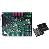
KIT35XS3400EVBE
Manufacturer Part Number
KIT35XS3400EVBE
Description
KIT EVALUATION FOR MC35XS3400
Manufacturer
Freescale Semiconductor
Specifications of KIT35XS3400EVBE
Main Purpose
Automotive Lighting
Utilized Ic / Part
*
Primary Attributes
4 protected high-side switches
Secondary Attributes
SPI Interface
Silicon Manufacturer
Freescale
Silicon Core Number
MC35XS3400
Kit Application Type
Power Management
Application Sub Type
EXtreme Switch
Kit Contents
Evaluation Board, CD
Rohs Compliant
Yes
Lead Free Status / RoHS Status
Lead free / RoHS Compliant
Embedded
-
Lead Free Status / Rohs Status
Lead free / RoHS Compliant


Table 4. Static Electrical Characteristics (continued)
otherwise noted. Typical values noted reflect the approximate parameter means at T
otherwise noted.
10
35XS3400
ELECTRICAL CHARACTERISTICS
STATIC ELECTRICAL CHARACTERISTICS
CONTROL INTERFACE
Notes
Input Logic High Voltage
Input Logic Low Voltage
Input Logic Pull-down Current (SCLK, SI)
Input Logic Pull-up Current (
SO,
Input Logic Pull-down Resistor (
Input Capacitance
Wake Input Clamp Voltage
Wake Input Forward Voltage
SO High State Output Voltage
SO and
SO, CSNS and
FSI External Pull-down Resistance
20.
21.
22.
23.
24.
25.
Characteristics noted under conditions 6.0 V ≤ V
I
I
I
CS
Watchdog Disabled
Watchdog Enabled
CL(WAKE)
OH
OL
FS
Upper and lower logic threshold voltage range applies to SI,
signals may be supplied by a derived voltage referenced to V
Input capacitance of SI,
tested.
The current must be limited by a series resistance when using voltages > 7.0 V.
Pull-down current is with V
Pull-up current is with V
In Fail-Safe HS[0:3] depends respectively on ON[0:3]. FSI has an active internal pull-up to V
= V
= -1.0 mA
= 1.0 mA
Tri-state Capacitance
FS
IH
Low-state Output Voltage
and 0 V < V
= -2.5 mA
FS
(21)
Tri-state Leakage Current
(20)
SO
(20)
(22)
Characteristic
< V
CS
(21)
,
CS
CS
DD
)
I
(24)
RST
CL(WAKE)
SI
< 2.0 V.
, SCLK,
, or
(25)
> 1.0 V and V
, WAKE and IN[0:3])
FS
= 5.5 V, or CSNS=0.0 V
(23)
CS
< 2.5 mA
RST
has an active internal pull-up to V
, IN[0:3] and WAKE. This parameter is guaranteed by process monitoring but is not production
SCLK
> 1.0 V.
PWR
35XS3400C
35XS3400D
≤ 20 V, 3.0 V ≤ V
CS
PWR
, SCLK,
.
V
V
I
SO(LEAK)
Symbol
CL(WAKE)
F(WAKE)
R
V
I
V
RST
C
RFS
DD
DWN
V
C
V
I
DWN
SOH
SOL
UP
DD
SO
IH
IN
IL
.
, IN[0:3] and WAKE input signals. The WAKE and
≤ 5.5 V, - 40°C ≤ T
V
A
DD
- 2.0
- 2.0
Min
-0.3
125
= 25°C under nominal conditions, unless
2.0
5.0
5.0
18
20
10
–
–
–
–
-0.4
REG
Analog Integrated Circuit Device Data
~ 3.0 V.
A
Infinite
≤ 125°C, GND = 0 V, unless
Typ
250
4.0
25
27
–
–
–
–
–
–
–
–
0
0
Freescale Semiconductor
V
DD
Max
500
- 0.3
0.8
0.4
2.0
1.0
20
20
20
12
32
35
–
–
+0.3
Unit
RST
μA
μA
pF
kΩ
pF
μA
kΩ
V
V
V
V
V
V
Related parts for KIT35XS3400EVBE
Image
Part Number
Description
Manufacturer
Datasheet
Request
R

Part Number:
Description:
Manufacturer:
Freescale Semiconductor, Inc
Datasheet:
Part Number:
Description:
Manufacturer:
Freescale Semiconductor, Inc
Datasheet:
Part Number:
Description:
Manufacturer:
Freescale Semiconductor, Inc
Datasheet:
Part Number:
Description:
Manufacturer:
Freescale Semiconductor, Inc
Datasheet:
Part Number:
Description:
Manufacturer:
Freescale Semiconductor, Inc
Datasheet:
Part Number:
Description:
Manufacturer:
Freescale Semiconductor, Inc
Datasheet:
Part Number:
Description:
Manufacturer:
Freescale Semiconductor, Inc
Datasheet:
Part Number:
Description:
Manufacturer:
Freescale Semiconductor, Inc
Datasheet:
Part Number:
Description:
Manufacturer:
Freescale Semiconductor, Inc
Datasheet:
Part Number:
Description:
Manufacturer:
Freescale Semiconductor, Inc
Datasheet:
Part Number:
Description:
Manufacturer:
Freescale Semiconductor, Inc
Datasheet:
Part Number:
Description:
Manufacturer:
Freescale Semiconductor, Inc
Datasheet:
Part Number:
Description:
Manufacturer:
Freescale Semiconductor, Inc
Datasheet:
Part Number:
Description:
Manufacturer:
Freescale Semiconductor, Inc
Datasheet:
Part Number:
Description:
Manufacturer:
Freescale Semiconductor, Inc
Datasheet: