KIT35XS3400EVBE Freescale Semiconductor, KIT35XS3400EVBE Datasheet - Page 25
KIT35XS3400EVBE
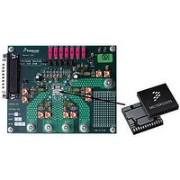
Manufacturer Part Number
KIT35XS3400EVBE
Description
KIT EVALUATION FOR MC35XS3400
Manufacturer
Freescale Semiconductor
Specifications of KIT35XS3400EVBE
Main Purpose
Automotive Lighting
Utilized Ic / Part
*
Primary Attributes
4 protected high-side switches
Secondary Attributes
SPI Interface
Silicon Manufacturer
Freescale
Silicon Core Number
MC35XS3400
Kit Application Type
Power Management
Application Sub Type
EXtreme Switch
Kit Contents
Evaluation Board, CD
Rohs Compliant
Yes
Lead Free Status / RoHS Status
Lead free / RoHS Compliant
Embedded
-
Lead Free Status / Rohs Status
Lead free / RoHS Compliant


FAIL-SAFE MODE
Watchdog
detection is active when either the WAKE or IN_ON[0:3] or
RST
input is capable of being pulled up to VPWR with a series of
limiting resistance limiting the internal clamp current
according to the specification.
As long as the WD bit (D15) of an incoming SPI message is
toggled within the minimum watchdog timeout period
(WDTO), the device will operate normally.
Fail-safe Conditions
for FSI open
(V
device will revert to a Fail-safe mode until the WD bit is written
to logic [1] (see fail-safe to normal mode transition paragraph)
and V
corresponding input. The SPI register content is reset to their
default value (except POR bit) and fault protections are fully
operational.
bit is set to [0].
NORMAL & FAIL-SAFE MODE TRANSITIONS
voltage and the microcontroller has to send a SPI command
with WDIN bit set to logic [1]; the other bits are not
considered. The previous latched faults are reset by the
transition into Normal mode (autoretry included).
mode due to watchdog timeout issue by forcing the FSI pin to
logic [0].
Transition Fail-Safe to Normal mode
Analog Integrated Circuit Device Data
Freescale Semiconductor
Table 9. SPI Watchdog Activation
0 (shorted to ground)
DD
The 35XS3400 is in Fail-safe mode when:
• V
• wake-up = 1,
• fail = 1,
• fault = 0.
If the FSI input is not grounded, the watchdog timeout
The watchdog timeout is a multiple of an internal oscillator.
If an internal watchdog time-out occurs before the WD bit
During the Fail-safe mode, the outputs will depend on the
The Fail-safe mode can be detected by monitoring the NM
To leave the Fail-safe mode, V
Moreover, the device can be brought out of the Fail-safe
Typical RFSI (Ω)
input pin transitions from logic [0] to logic [1]. The WAKE
< V
DD
PWR
(open)
DD(FAIL)
is within the normal voltage range.
is within the normal voltage range,
(Table
)) for VDD_FAIL_en bit is set to logic [1], the
9) or in case of V
DD
Watchdog
Disabled
must be in nominal
Enable
DD
failure condition
occurred (fail=1). The previous latched faults are reset by the
transition into Fail-safe mode (autoretry included).
FAULT MODE
driving the
fault condition is removed, except for over-current, severe
short-circuit, over-temperature and under-voltage which will
be reset by a new turn-on command (each fault_control
signal to be toggled).
available (and reset) via the SO pin during the first valid SPI
communication.
SPI register without effect on the corresponding output state
(HS[x]) and the
START-UP SEQUENCE
following sequence is provided:
set to logic [1]) with an external reference clock:
function is not guaranteed.
Transition Normal to Fail-safe Mode
To leave the Normal mode, a fail-safe condition must
The 35XS3400 is in Fault mode when:
• V
• wake-up = 1,
• fail = X,
• fault=1.
This device indicates the faults below as they occur by
•Over-temperature fault,
•Over-current fault,
•Severe short-circuit fault,
•Output(s) shorted to VPWR fault in OFF state,
•Open load fault in OFF state,
•Over-voltage fault (enabled by default),
•Under-voltage fault.
The
Fault information is retained in the SPI fault register and is
The Open load fault in ON state is only reported through
The 35XS3400 enters in Normal mode after start-up if
•VPWR and VDD power supplies must be above their
•generate wake-up event (wake-up=1) from 0 to 1 on
And, in case of the PWM module is used (PWM_en bit is
•apply PWM clock on IN0 input pin after maximum 200 μs
If the correct start-up sequence is not provided, the PWM
under-voltage thresholds,
RSTB. The device switches to Normal mode with SPI
register content is reset (as defined in
Table
after 50μs typical and all SPI registers are set to default
values (set to logic [0]). The UV fault is reported in the
SPI status registers.
(min. 50 μs).
PWR
FS
pin will automatically return to logic [1] when the
FS
23). All features of 35XS3400 will be available
and V
pin to logic [0] for RST input is pulled up:
FS
DD
pin.
are within the normal voltage range,
FUNCTIONAL DEVICE OPERATION
OPERATIONAL MODES
Table 11
35XS3400
and
25
Related parts for KIT35XS3400EVBE
Image
Part Number
Description
Manufacturer
Datasheet
Request
R

Part Number:
Description:
Manufacturer:
Freescale Semiconductor, Inc
Datasheet:
Part Number:
Description:
Manufacturer:
Freescale Semiconductor, Inc
Datasheet:
Part Number:
Description:
Manufacturer:
Freescale Semiconductor, Inc
Datasheet:
Part Number:
Description:
Manufacturer:
Freescale Semiconductor, Inc
Datasheet:
Part Number:
Description:
Manufacturer:
Freescale Semiconductor, Inc
Datasheet:
Part Number:
Description:
Manufacturer:
Freescale Semiconductor, Inc
Datasheet:
Part Number:
Description:
Manufacturer:
Freescale Semiconductor, Inc
Datasheet:
Part Number:
Description:
Manufacturer:
Freescale Semiconductor, Inc
Datasheet:
Part Number:
Description:
Manufacturer:
Freescale Semiconductor, Inc
Datasheet:
Part Number:
Description:
Manufacturer:
Freescale Semiconductor, Inc
Datasheet:
Part Number:
Description:
Manufacturer:
Freescale Semiconductor, Inc
Datasheet:
Part Number:
Description:
Manufacturer:
Freescale Semiconductor, Inc
Datasheet:
Part Number:
Description:
Manufacturer:
Freescale Semiconductor, Inc
Datasheet:
Part Number:
Description:
Manufacturer:
Freescale Semiconductor, Inc
Datasheet:
Part Number:
Description:
Manufacturer:
Freescale Semiconductor, Inc
Datasheet: