KIT35XS3400EVBE Freescale Semiconductor, KIT35XS3400EVBE Datasheet - Page 20
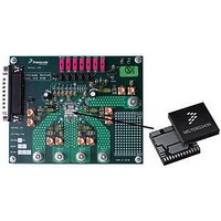
KIT35XS3400EVBE
Manufacturer Part Number
KIT35XS3400EVBE
Description
KIT EVALUATION FOR MC35XS3400
Manufacturer
Freescale Semiconductor
Specifications of KIT35XS3400EVBE
Main Purpose
Automotive Lighting
Utilized Ic / Part
*
Primary Attributes
4 protected high-side switches
Secondary Attributes
SPI Interface
Silicon Manufacturer
Freescale
Silicon Core Number
MC35XS3400
Kit Application Type
Power Management
Application Sub Type
EXtreme Switch
Kit Contents
Evaluation Board, CD
Rohs Compliant
Yes
Lead Free Status / RoHS Status
Lead free / RoHS Compliant
Embedded
-
Lead Free Status / Rohs Status
Lead free / RoHS Compliant


GROUND (GND)
POSITIVE POWER SUPPLY (VPWR)
source of operational power for the device. The VPWR
contact is the backside surface mount tab of the package.
SERIAL OUTPUT (SO)
register. The SO pin remains in a high-impedance state until
the
of reporting the status of the output, the device configuration,
the state of the key inputs, etc. The SO pin changes state on
the rising edge of SCLK and reads out on the falling edge of
POWER SUPPLY
on the VPWR pin. Characteristics are provided from 6.0 V to
20 V for the device. The VPWR pin supplies power to internal
regulator, analog, and logic circuit blocks. The VDD supply is
used for Serial Peripheral Interface (SPI) communication in
order to configure and diagnose the device. This IC
architecture provides a low quiescent current Sleep mode.
Applying V
the Normal mode. The device will transit to Fail-safe mode in
case of failures on the SPI or/and on VDD voltage.
HIGH SIDE SWITCHES: HS0 – HS3
automotive lamps located for the rear of vehicle, such as
20
35XS3400
FUNCTIONAL DESCRIPTION
FUNCTIONAL INTERNAL BLOCK DESCRIPTION
These pins are the ground for the device.
This pin connects to the positive power supply and is the
The SO data pin is a tri-stateable output from the shift
The 35XS3400 is designed to operate from 4.0 V to 28 V
These pins are the high side outputs controlling
CS
pin is put into a logic [0] state. The SO data is capable
PWR
and V
DD
to the device will place the device in
INTERFACE
FUNCTIONAL INTERNAL BLOCK DESCRIPTION
MCU
PARALLEL CONTROL
MCU INTERFACE and
PWM CONTROLLER
OUTPUT CONTROL
POWER SUPPLY
SPI INTERFACE
INPUTS
SCLK. SO reporting descriptions are provided in
page 35.
HIGH SIDE OUTPUTS (HS3, HS1, HS0, HS2)
FAIL-SAFE INPUT (FSI)
source from internal supply (V
watchdog timeout feature.
enabled. After a watchdog timeout occurs, the output states
depends on IN[0:3].
circuit is disabled. The output states depends on IN[0:3] in
case of V
activated (VDD_FAIL_en bit sets to logic [1]).
28 W bulbs and LED modules. 55 W/65 W lamps can be
driven for two outputs shorted together. Those N-channel
MOSFETs with 35 mΩ R
present extended diagnostics in order to detect bulb outage
and short-circuit fault condition. The HS output is actively
clamped during turn off of inductive loads and inductive
battery line.
multiple switching, an external recirculation device must be
used to maintain the device in its Safe Operating Area.
MCU INTERFACE AND OUTPUT CONTROL
MCU through SPI. A pulse width modulation control module
allows improvement of lamp lifetime with bulb power
Protected 35 mΩ high side power outputs to the load.
This pin incorporates an active internal pull-up current
When the FSI pin is opened, the watchdog circuit is
When the FSI pin is connected to GND, the watchdog
When driving DC motor or solenoid loads demanding
In Normal mode, each bulb is controlled directly from the
DD
PROTECTED
failure condition, in case V
SWITCHES
HIGH SIDE
HS0-HS3
SELF-
Analog Integrated Circuit Device Data
DS(ON)
REG
are self-protected and
). This enables the
Freescale Semiconductor
DD
failure detection is
Table
23,
Related parts for KIT35XS3400EVBE
Image
Part Number
Description
Manufacturer
Datasheet
Request
R

Part Number:
Description:
Manufacturer:
Freescale Semiconductor, Inc
Datasheet:
Part Number:
Description:
Manufacturer:
Freescale Semiconductor, Inc
Datasheet:
Part Number:
Description:
Manufacturer:
Freescale Semiconductor, Inc
Datasheet:
Part Number:
Description:
Manufacturer:
Freescale Semiconductor, Inc
Datasheet:
Part Number:
Description:
Manufacturer:
Freescale Semiconductor, Inc
Datasheet:
Part Number:
Description:
Manufacturer:
Freescale Semiconductor, Inc
Datasheet:
Part Number:
Description:
Manufacturer:
Freescale Semiconductor, Inc
Datasheet:
Part Number:
Description:
Manufacturer:
Freescale Semiconductor, Inc
Datasheet:
Part Number:
Description:
Manufacturer:
Freescale Semiconductor, Inc
Datasheet:
Part Number:
Description:
Manufacturer:
Freescale Semiconductor, Inc
Datasheet:
Part Number:
Description:
Manufacturer:
Freescale Semiconductor, Inc
Datasheet:
Part Number:
Description:
Manufacturer:
Freescale Semiconductor, Inc
Datasheet:
Part Number:
Description:
Manufacturer:
Freescale Semiconductor, Inc
Datasheet:
Part Number:
Description:
Manufacturer:
Freescale Semiconductor, Inc
Datasheet:
Part Number:
Description:
Manufacturer:
Freescale Semiconductor, Inc
Datasheet: