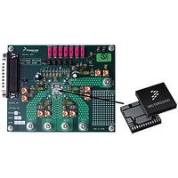
KIT35XS3400EVBE Freescale Semiconductor, KIT35XS3400EVBE Datasheet - Page 33

KIT35XS3400EVBE
Manufacturer Part Number
KIT35XS3400EVBE
Description
KIT EVALUATION FOR MC35XS3400
Manufacturer
Freescale Semiconductor
Specifications of KIT35XS3400EVBE
Main Purpose
Automotive Lighting
Utilized Ic / Part
*
Primary Attributes
4 protected high-side switches
Secondary Attributes
SPI Interface
Silicon Manufacturer
Freescale
Silicon Core Number
MC35XS3400
Kit Application Type
Power Management
Application Sub Type
EXtreme Switch
Kit Contents
Evaluation Board, CD
Rohs Compliant
Yes
Lead Free Status / RoHS Status
Lead free / RoHS Compliant
Embedded
-
Lead Free Status / Rohs Status
Lead free / RoHS Compliant
ADDRESS A
REGISTER (OCR)
corresponding output over-current protection through the
SPI. Each output “s” is independently selected for
configuration based on the state of the D14 : D13 bits
(Table
curve and D[5:4] bits inrush curve for selected output, as
shown
.
replaced by OCHI2 during t
Table 15. Current Sense Ratio Selection
Analog Integrated Circuit Device Data
Freescale Semiconductor
Table 16. Cooling and Inrush Curve Selection
Table 17. Inrush Curve Selection
The OCR_s register allows the MCU to configure
D[7:6] bits allow to MCU to programmable bulb cooling
A logic [1] on bit D3 (OCHI_s bit) the OCHI1 level is
BC1_s (D7)
OC1_s (D5)
CSNS_high_s (D0)
12).
Table 16
0
0
1
1
0
0
1
1
0
1
1
A
and
0
100 — OUTPUT OVER-CURRENT
Table
BC0_s (D6)
OC0_s (D4)
17.
0
1
0
1
OC1
0
1
0
1
, as shown
Current Sense Ratio
Profile Curves Speed
CRS0 (default)
Profile Curves Speed
medium (default)
CRS1
Figure
slow (default)
medium
very slow
medium
slow
fast
fast
13.
current levels in steady state, as defined in
mode, as described
ADDRESS 00101 — GLOBAL CONFIGURATION
REGISTER (GCR)
through the SPI.
detector. A logic [1] on VDD_FAIL_en bit allows transitioning
to Fail-safe mode for V
module. A logic [1] on PWM_en bit allows control of the
outputs HS[0:3] with PWMR register (the direct input states
are ignored).
reference by PWM module, as described in the following
Table
Table 19. Over-current Mode Selection
OC_mode_s (D0)
I
I
I
I
I
I
I
I
I
I
Figure 13. Over-current profile with OCHI bit set to ‘1’
OCH
OCH2
OC1
OC2
OC3
OC4
OCLO4
OCLO3
OCLO2
OCLO1
Table 18. Output Steady State Selection
OCLO1 (D2) OCLO0 (D1)
The wire harness is protected by one of four possible
Bit D0 (OC_mode_sel) allows to select the over-current
The GCR register allows the MCU to configure the device
Bit D8 allows the MCU to enable or disable the V
Bit D7 allows the MCU to enable or disable the PWM
Bit D6 (CLOCK_sel) allows to select the clock used as
1
20.
t
OC1
0
0
1
1
0
1
t
OC2
t
OC3
t
OC4
inrush current and bulb cooling management
0
1
0
1
Table
only inrush current management (default)
DD
t
LOGIC COMMANDS AND REGISTERS
OC5
< V
FUNCTIONAL DEVICE OPERATION
19.
DD(FAIL).
Over-current Mode
t
OC6
Steady State Current
OCLO2 (default)
OCLO3
OCLO4
OCLO1
t
OC7
Table
18.
Time
DD
35XS3400
failure
33


