KIT35XS3400EVBE Freescale Semiconductor, KIT35XS3400EVBE Datasheet - Page 22
KIT35XS3400EVBE
Manufacturer Part Number
KIT35XS3400EVBE
Description
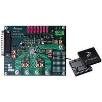
KIT EVALUATION FOR MC35XS3400
Manufacturer
Freescale Semiconductor
Specifications of KIT35XS3400EVBE
Main Purpose
Automotive Lighting
Utilized Ic / Part
*
Primary Attributes
4 protected high-side switches
Secondary Attributes
SPI Interface
Silicon Manufacturer
Freescale
Silicon Core Number
MC35XS3400
Kit Application Type
Power Management
Application Sub Type
EXtreme Switch
Kit Contents
Evaluation Board, CD
Rohs Compliant
Yes
Lead Free Status / RoHS Status
Lead free / RoHS Compliant
Embedded
-
Lead Free Status / Rohs Status
Lead free / RoHS Compliant


SPI PROTOCOL DESCRIPTION
synchronous data transfer with four I/O lines associated with
it: Serial Input (SI), Serial Output (SO), Serial Clock (SCLK),
and Chip Select (
22
35XS3400
FUNCTIONAL DEVICE OPERATION
FUNCTIONAL INTERNAL BLOCK DESCRIPTION
The SPI interface has a full duplex, three-wire
CSB
SCLK
CS
SO
SI
NOTES:
Notes
CS
D15
1.
2.
OD15
).
1.
2. D15
3. OD15
RSTB is in a logic H state during the above operation.
DO, D1, D2, ... , and D15 relate to the most recent ordered entry of program data into the LUX IC
RST
D14
OD14
:
is a logic [1] state during the above operation.
D0 relate to the most recent ordered entry of data into the device.
:
OD0 relate to the first 16 bits of ordered fault and status data out of the device.
D13
OD13
D12
OD12
Figure 9. Single 16-Bit Word SPI Communication
FUNCTIONAL DEVICE OPERATION
D11
OD11
CS
D10
OD10
D9
OD9
D8
OD8
(D15 to D0) protocol, with both input and output words
transferring the most significant bit (MSB) first. All inputs are
compatible with 5.0 V or 3.3 V CMOS logic levels.
D7
OD7
The SI / SO pins of the 35XS3400 follow a first-in first-out
D6
OD6
D5
OD5
D4
OD4
device.
Analog Integrated Circuit Device Data
D3
OD3
D2
OD2
Freescale Semiconductor
D1
OD1
D0
OD0
Related parts for KIT35XS3400EVBE
Image
Part Number
Description
Manufacturer
Datasheet
Request
R

Part Number:
Description:
Manufacturer:
Freescale Semiconductor, Inc
Datasheet:
Part Number:
Description:
Manufacturer:
Freescale Semiconductor, Inc
Datasheet:
Part Number:
Description:
Manufacturer:
Freescale Semiconductor, Inc
Datasheet:
Part Number:
Description:
Manufacturer:
Freescale Semiconductor, Inc
Datasheet:
Part Number:
Description:
Manufacturer:
Freescale Semiconductor, Inc
Datasheet:
Part Number:
Description:
Manufacturer:
Freescale Semiconductor, Inc
Datasheet:
Part Number:
Description:
Manufacturer:
Freescale Semiconductor, Inc
Datasheet:
Part Number:
Description:
Manufacturer:
Freescale Semiconductor, Inc
Datasheet:
Part Number:
Description:
Manufacturer:
Freescale Semiconductor, Inc
Datasheet:
Part Number:
Description:
Manufacturer:
Freescale Semiconductor, Inc
Datasheet:
Part Number:
Description:
Manufacturer:
Freescale Semiconductor, Inc
Datasheet:
Part Number:
Description:
Manufacturer:
Freescale Semiconductor, Inc
Datasheet:
Part Number:
Description:
Manufacturer:
Freescale Semiconductor, Inc
Datasheet:
Part Number:
Description:
Manufacturer:
Freescale Semiconductor, Inc
Datasheet:
Part Number:
Description:
Manufacturer:
Freescale Semiconductor, Inc
Datasheet: