KIT35XS3400EVBE Freescale Semiconductor, KIT35XS3400EVBE Datasheet - Page 6
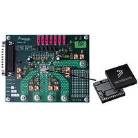
KIT35XS3400EVBE
Manufacturer Part Number
KIT35XS3400EVBE
Description
KIT EVALUATION FOR MC35XS3400
Manufacturer
Freescale Semiconductor
Specifications of KIT35XS3400EVBE
Main Purpose
Automotive Lighting
Utilized Ic / Part
*
Primary Attributes
4 protected high-side switches
Secondary Attributes
SPI Interface
Silicon Manufacturer
Freescale
Silicon Core Number
MC35XS3400
Kit Application Type
Power Management
Application Sub Type
EXtreme Switch
Kit Contents
Evaluation Board, CD
Rohs Compliant
Yes
Lead Free Status / RoHS Status
Lead free / RoHS Compliant
Embedded
-
Lead Free Status / Rohs Status
Lead free / RoHS Compliant


Table 3. Maximum Ratings
permanent damage to the device.
6
35XS3400
ELECTRICAL CHARACTERISTICS
MAXIMUM RATINGS
ELECTRICAL RATINGS
THERMAL RATINGS
THERMAL RESISTANCE
Notes
V
V
Input / Output Voltage
WAKE Input Clamp Current
CSNS Input Clamp Current
HS [0:3] Voltage
Output Current
Output Clamp Energy using single-pulse method
ESD Voltage
Operating Temperature
Storage Temperature
Thermal Resistance
Peak Package Reflow Temperature During Reflow
All voltages are with respect to ground unless otherwise noted. Exceeding these ratings may cause a malfunction or
PWR
DD
3.
4.
5.
6.
7.
8.
9.
Load Dump at 25°C (400 ms)
Maximum Operating Voltage
Reverse Battery at 25°C (2.0 min.)
Positive
Negative
Human Body Model (HBM) for HS[0:3], VPWR and GND
Human Body Model (HBM) for other pins
Charge Device Model (CDM)
Ambient
Junction
Junction to Case
Junction to Ambient
Supply Voltage Range
Continuous high side output current rating so long as maximum junction temperature is not exceeded. Calculation of maximum output
current using package thermal resistance is required.
Active clamp energy using single-pulse method (L = 2.0 mH, R
ESD testing is performed in accordance with the Human Body Model (HBM) (C
(C
Input / Output pins are: IN[0:3], RST, FSI, CSNS, SI, SCLK, CS, SO, FS
Device mounted on a 2s2p test board per JEDEC JESD51-2. 15 °C/W of R
Pin soldering temperature limit is for 10 seconds maximum duration. Not designed for immersion soldering. Exceeding these limits may
cause malfunction or permanent damage to the device.
Freescale’s Package Reflow capability meets Pb-free requirements for JEDEC standard J-STD-020C. For Peak Package Reflow
Temperature and Moisture Sensitivity Levels (MSL), Go to www.freescale.com, search by part number [e.g. remove prefixes/suffixes
and enter the core ID to view all orderable parts (i.e. MC33xxxD enter 33xxx), and review parametrics.
Supply Voltage Range
Corner Pins (1, 13, 19, 21)
All Other Pins (2-12, 14-18, 20, 22-24)
ZAP
(5)
= 200 pF, R
(3)
(7)
ZAP
= 0 Ω), and the Charge Device Model (CDM), Robotic (C
Ratings
ELECTRICAL CHARACTERISTICS
(4)
(8)
,
(9)
MAXIMUM RATINGS
L
= 0 Ω, V
PWR
θJA
can be reached in a real application case (4 layers board).
= 14 V, T
ZAP
I
V
I
CL(WAKE)
CL(CSNS)
Symbol
V
E
ZAP
I
PWR(SS)
V
V
V
V
T
HS[0:3]
T
HS[0:3]
CL [0:3]
R
R
V
ESD1
ESD2
ESD3
ESD4
PPRT
T
T
STG
= 100 pF, R
(6)
θ
θ
DD
A
J
JC
JA
= 4.0 pF).
J
= 150
Analog Integrated Circuit Device Data
ZAP
°
C initial).
-0.3 to V
= 1500 Ω), the Machine Model (MM)
-0.3 to 5.5
- 40 to 125
- 40 to 150
- 55 to 150
± 8000
± 2000
Value
Note 9
± 750
± 500
<1.0
-18
-16
2.5
2.5
41
28
41
35
30
6
DD
Freescale Semiconductor
+ 0.3
°
Unit
mA
mA
C/ W
mJ
°
°
°C
V
V
V
V
A
V
C
C
Related parts for KIT35XS3400EVBE
Image
Part Number
Description
Manufacturer
Datasheet
Request
R

Part Number:
Description:
Manufacturer:
Freescale Semiconductor, Inc
Datasheet:
Part Number:
Description:
Manufacturer:
Freescale Semiconductor, Inc
Datasheet:
Part Number:
Description:
Manufacturer:
Freescale Semiconductor, Inc
Datasheet:
Part Number:
Description:
Manufacturer:
Freescale Semiconductor, Inc
Datasheet:
Part Number:
Description:
Manufacturer:
Freescale Semiconductor, Inc
Datasheet:
Part Number:
Description:
Manufacturer:
Freescale Semiconductor, Inc
Datasheet:
Part Number:
Description:
Manufacturer:
Freescale Semiconductor, Inc
Datasheet:
Part Number:
Description:
Manufacturer:
Freescale Semiconductor, Inc
Datasheet:
Part Number:
Description:
Manufacturer:
Freescale Semiconductor, Inc
Datasheet:
Part Number:
Description:
Manufacturer:
Freescale Semiconductor, Inc
Datasheet:
Part Number:
Description:
Manufacturer:
Freescale Semiconductor, Inc
Datasheet:
Part Number:
Description:
Manufacturer:
Freescale Semiconductor, Inc
Datasheet:
Part Number:
Description:
Manufacturer:
Freescale Semiconductor, Inc
Datasheet:
Part Number:
Description:
Manufacturer:
Freescale Semiconductor, Inc
Datasheet:
Part Number:
Description:
Manufacturer:
Freescale Semiconductor, Inc
Datasheet: