KIT35XS3400EVBE Freescale Semiconductor, KIT35XS3400EVBE Datasheet - Page 34
KIT35XS3400EVBE
Manufacturer Part Number
KIT35XS3400EVBE
Description
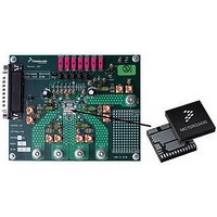
KIT EVALUATION FOR MC35XS3400
Manufacturer
Freescale Semiconductor
Specifications of KIT35XS3400EVBE
Main Purpose
Automotive Lighting
Utilized Ic / Part
*
Primary Attributes
4 protected high-side switches
Secondary Attributes
SPI Interface
Silicon Manufacturer
Freescale
Silicon Core Number
MC35XS3400
Kit Application Type
Power Management
Application Sub Type
EXtreme Switch
Kit Contents
Evaluation Board, CD
Rohs Compliant
Yes
Lead Free Status / RoHS Status
Lead free / RoHS Compliant
Embedded
-
Lead Free Status / Rohs Status
Lead free / RoHS Compliant


feedback on CSNS output pin, as shown in
(D0). When this bits is [0], the over-voltage is enabled (default
value).
ADDRESS 00111 — CALIBRATION REGISTER
(CALR)
clock, as explained in
SERIAL OUTPUT COMMUNICATION (DEVICE
STATUS RETURN DATA)
loaded. Meanwhile, the data is clocked out MSB- (OD15-)
first as the new message data is clocked into the SI pin. The
first sixteen bits of data clocking out of the SO, and following
34
35XS3400
Table 21. CSNS Reporting Selection
FUNCTIONAL DEVICE OPERATION
LOGIC COMMANDS AND REGISTERS
Table 22. Output Current Recopy Selection
TEMP_en
Table 20. PWM Module Selection
CSNS1 (D3)
PWM_en (D7) CLOCK_sel (D6)
Bits D5:D4 allow the MCU to select one of two analog
The GCR register disables the over-voltage protection
The CALR register allows the MCU to calibrate internal
When the
(D5)
X
0
1
0
0
1
1
0
1
1
CSNS_en
CS
(D4)
CSNS0 (D2)
0
1
0
pin is pulled low, the output register is
0
1
0
1
current recopy of selected output (D3:2] bits)
Figure
X
0
1
12.
temperature on GND flag
CSNS tri-stated (default)
CSNS reporting
PWM module enabled with
PWM module enabled with
internal calibrated clock
external clock from IN0
PWM module disabled
CSNS reporting
HS0 (default)
PWM module
HS1
HS2
HS3
(default)
Table
21.
a
word.
first 16 bits will be representative of the initial message bits
clocked into the SI pin since the
logic [0]. This feature is useful for daisy-chaining devices as
well as message verification.
transition of [0] to [1]. If there is a valid message length, the
data is latched into the appropriate registers. A valid
message length is a multiple of 16 bits. At this time, the SO
pin is tri-stated and the fault status register is now able to
accept new fault status information.
status to register contents, user selected by writing to the
STATR bits OD4, OD3, OD2, OD1, and OD0. The value of
the previous bits SOA4 and SOA3 will determine which
output the SO information applies to for the registers which
are output specific; viz., Fault, PWMR, CONFR0, CONFR1
and OCR registers.
information for each output (depending on the previous
SOA4, SOA3 state) that was selected during the most recent
STATR write until changed with an updated STATR write.
the STATR-selected register data at the time that the
pulled to a logic [0] during SPI communication, and/or for the
period of time since the last valid SPI communication, with
the following exception:
SERIAL OUTPUT BIT ASSIGNMENT
serial input message, as explained in the following
paragraphs.
OD15 : OD0.
CS
Any bits clocked out of the Serial Output (SO) pin after the
A valid message length is determined following a
SO data will represent information ranging from fault
Note that the SO data will continue to reflect the
The output status register correctly reflects the status of
•The previous SPI communication was determined to be
•The VPWR voltage is below 4.0 V, the status must be
The 16 bits of serial output data depend on the previous
• Bit OD15 is the MSB; it reflects the state of the
• Bits OD14:OD10 reflect the state of the bits
• Bit OD9 is set to logic [1] in Normal mode (NM).
• The contents of bits OD8 : OD0 depend on bits D4 : D0
transition, is dependent upon the previously written SPI
invalid. In this case, the status will be reported as
though the invalid SPI communication never occurred.
ignored by the MCU.
Watchdog bit from the previously clocked-in message.
SOA4 : SOA0 from the previously clocked in message.
from the most recent STATR command SOA4 : SOA0
as explained in the paragraphs following
Table
23, summarizes SO returned data for bits
Analog Integrated Circuit Device Data
CS
Freescale Semiconductor
pin first transitioned to a
Table
CS
23.
CS
is
Related parts for KIT35XS3400EVBE
Image
Part Number
Description
Manufacturer
Datasheet
Request
R

Part Number:
Description:
Manufacturer:
Freescale Semiconductor, Inc
Datasheet:
Part Number:
Description:
Manufacturer:
Freescale Semiconductor, Inc
Datasheet:
Part Number:
Description:
Manufacturer:
Freescale Semiconductor, Inc
Datasheet:
Part Number:
Description:
Manufacturer:
Freescale Semiconductor, Inc
Datasheet:
Part Number:
Description:
Manufacturer:
Freescale Semiconductor, Inc
Datasheet:
Part Number:
Description:
Manufacturer:
Freescale Semiconductor, Inc
Datasheet:
Part Number:
Description:
Manufacturer:
Freescale Semiconductor, Inc
Datasheet:
Part Number:
Description:
Manufacturer:
Freescale Semiconductor, Inc
Datasheet:
Part Number:
Description:
Manufacturer:
Freescale Semiconductor, Inc
Datasheet:
Part Number:
Description:
Manufacturer:
Freescale Semiconductor, Inc
Datasheet:
Part Number:
Description:
Manufacturer:
Freescale Semiconductor, Inc
Datasheet:
Part Number:
Description:
Manufacturer:
Freescale Semiconductor, Inc
Datasheet:
Part Number:
Description:
Manufacturer:
Freescale Semiconductor, Inc
Datasheet:
Part Number:
Description:
Manufacturer:
Freescale Semiconductor, Inc
Datasheet:
Part Number:
Description:
Manufacturer:
Freescale Semiconductor, Inc
Datasheet: