KIT35XS3400EVBE Freescale Semiconductor, KIT35XS3400EVBE Datasheet - Page 15
KIT35XS3400EVBE
Manufacturer Part Number
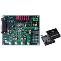
KIT35XS3400EVBE
Description
KIT EVALUATION FOR MC35XS3400
Manufacturer
Freescale Semiconductor
Specifications of KIT35XS3400EVBE
Main Purpose
Automotive Lighting
Utilized Ic / Part
*
Primary Attributes
4 protected high-side switches
Secondary Attributes
SPI Interface
Silicon Manufacturer
Freescale
Silicon Core Number
MC35XS3400
Kit Application Type
Power Management
Application Sub Type
EXtreme Switch
Kit Contents
Evaluation Board, CD
Rohs Compliant
Yes
Lead Free Status / RoHS Status
Lead free / RoHS Compliant
Embedded
-
Lead Free Status / Rohs Status
Lead free / RoHS Compliant


Table 5. Dynamic Electrical Characteristics (continued)
otherwise noted. Typical values noted reflect the approximate parameter means at T
otherwise noted.
SPI INTERFACE CHARACTERISTICS
Notes
Analog Integrated Circuit Device Data
Freescale Semiconductor
TEMPERATURE ON THE GND FLAG
Thermal Prewarning Detection
Analog Temperature Feedback at T
Analog Temperature Feedback Derating with R
Maximum Frequency of SPI Operation
Required Low State Duration for
Rising Edge of
Rising Edge of
Falling Edge of
Required High State Duration of SCLK (Required Setup Time)
Required Low State Duration of SCLK (Required Setup Time)
Falling Edge of SCLK to Rising Edge of
SI to Falling Edge of SCLK (Required Setup Time)
Falling Edge of SCLK to SI (Required Setup Time)
SO Rise Time
SO Fall Time
SI,
SI,
Time from Rising Edge of
Time from Rising Edge of
35.
36.
37.
38.
39.
40.
41.
Characteristics noted under conditions 6.0 V ≤ V
C
C
CS
CS
L
L
, SCLK, Incoming Signal Rise Time
, SCLK, Incoming Signal Fall Time
= 80 pF
= 80 pF
Parameters guaranteed by design.
Value guaranteed per statistical analysis
RST
Maximum setup time required for the 35XS3400 is the minimum guaranteed time needed from the microcontroller.
Rise and Fall time of incoming SI,
Time required for output status data to be available for use at SO. 1.0 kΩ on pull-up on
Time required for output status data to be terminated at SO. 1.0 kΩ on pull-up on
low duration measured with outputs enabled and going to OFF or disabled condition.
CS
RST
CS
to Falling Edge of
to Rising Edge of SCLK (Required Setup Time)
to Falling Edge of
SCLK
SCLK
(35)
Characteristic
to SO Low Logic Level
to SO High Logic Level
RST
A
CS
(37)
= 25°C with R
(35)
CS
CS
CS
(Required Setup Time)
(39)
(39)
(Required Setup Time)
, and SCLK signals suggested for design consideration to prevent the occurrence of double pulsing.
(Required Setup Time)
CSNS
(39)
(39)
CSNS
=2.5 kΩ
(40)
(41)
PWR
=2.5 kΩ
(36)
≤ 20 V, 3.0 V ≤ V
(38)
(38)
(38)
(38)
(38)
(38)
DD
t
T
t
Symbol
t
t
DT
SI (HOLD)
t
WSCLKh
t
t
T
WSCLKl
SO(DIS)
t
SO(EN)
OTWAR
t
SI (SU)
t
WRST
t
t
f
LEAD
t
ENBL
t
FEED
t
RSO
LAG
FSO
≤ 5.5 V, - 40°C ≤ T
SPI
RSI
FSI
FEED
CS
CS
.
A
CS
DYNAMIC ELECTRICAL CHARACTERISTICS
= 25°C under nominal conditions, unless
1.15
Min
110
-3.5
.
10
–
–
–
–
–
–
–
–
–
–
–
–
–
–
–
A
ELECTRICAL CHARACTERISTICS
≤ 125°C, GND = 0 V, unless
1.20
Typ
125
-3.7
–
–
–
–
–
–
–
–
–
–
–
–
–
–
–
–
Max
1.25
-3.9
140
500
8.0
1.0
5.0
50
50
60
37
49
13
13
13
13
60
60
–
35XS3400
mV/°C
Unit
MHz
°C
μs
μs
μs
ns
ns
ns
ns
ns
ns
ns
ns
ns
ns
ns
ns
V
15
Related parts for KIT35XS3400EVBE
Image
Part Number
Description
Manufacturer
Datasheet
Request
R

Part Number:
Description:
Manufacturer:
Freescale Semiconductor, Inc
Datasheet:
Part Number:
Description:
Manufacturer:
Freescale Semiconductor, Inc
Datasheet:
Part Number:
Description:
Manufacturer:
Freescale Semiconductor, Inc
Datasheet:
Part Number:
Description:
Manufacturer:
Freescale Semiconductor, Inc
Datasheet:
Part Number:
Description:
Manufacturer:
Freescale Semiconductor, Inc
Datasheet:
Part Number:
Description:
Manufacturer:
Freescale Semiconductor, Inc
Datasheet:
Part Number:
Description:
Manufacturer:
Freescale Semiconductor, Inc
Datasheet:
Part Number:
Description:
Manufacturer:
Freescale Semiconductor, Inc
Datasheet:
Part Number:
Description:
Manufacturer:
Freescale Semiconductor, Inc
Datasheet:
Part Number:
Description:
Manufacturer:
Freescale Semiconductor, Inc
Datasheet:
Part Number:
Description:
Manufacturer:
Freescale Semiconductor, Inc
Datasheet:
Part Number:
Description:
Manufacturer:
Freescale Semiconductor, Inc
Datasheet:
Part Number:
Description:
Manufacturer:
Freescale Semiconductor, Inc
Datasheet:
Part Number:
Description:
Manufacturer:
Freescale Semiconductor, Inc
Datasheet:
Part Number:
Description:
Manufacturer:
Freescale Semiconductor, Inc
Datasheet: