KIT35XS3400EVBE Freescale Semiconductor, KIT35XS3400EVBE Datasheet - Page 32
KIT35XS3400EVBE
Manufacturer Part Number
KIT35XS3400EVBE
Description
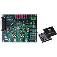
KIT EVALUATION FOR MC35XS3400
Manufacturer
Freescale Semiconductor
Specifications of KIT35XS3400EVBE
Main Purpose
Automotive Lighting
Utilized Ic / Part
*
Primary Attributes
4 protected high-side switches
Secondary Attributes
SPI Interface
Silicon Manufacturer
Freescale
Silicon Core Number
MC35XS3400
Kit Application Type
Power Management
Application Sub Type
EXtreme Switch
Kit Contents
Evaluation Board, CD
Rohs Compliant
Yes
Lead Free Status / RoHS Status
Lead free / RoHS Compliant
Embedded
-
Lead Free Status / Rohs Status
Lead free / RoHS Compliant


DEVICE REGISTER ADDRESSING
addresses (D[14:10]) and their impact on device operation.
ADDRESS XX000 — STATUS REGISTER
(STATR_S)
the various configuration register contents without disrupting
the device operation or the register contents. The register bits
D[4:0] determine the content of the first sixteen bits of SO
data. In addition to the device status, this feature provides the
ability to read the content of the PWMR_s, CONFR0_s,
CONFR1_s, OCR_s, GCR and CALR registers (Refer to the
section entitled
Return Data) on page
ADDRESS A
REGISTER (PWMR_S )
of corresponding output through the SPI. Each output “s” is
independently selected for configuration based on the state
of the D14 : D13 bits
corresponding output switch and a logic [0] turns it OFF (if IN
input is also pulled down). Bits D6:D0 set the output PWM
duty-cycle to one of 128 levels for PWM_en is set to logic [1],
as shown
ADDRESS A
REGISTER (CONFR0_S )
corresponding output switching through the SPI. Each output
“s” is independently selected for configuration based on the
state of the D14 : D13 bits
will enable the output for direct control. A logic [1] on bit D5
will disable the output from direct control (in this case, the
output is only controlled by On bit).
or medium or low speed slew rate for the selected output, the
default value [00] corresponds to the medium speed slew rate
(Table
32
35XS3400
Table 12. Output Selection
FUNCTIONAL DEVICE OPERATION
LOGIC COMMANDS AND REGISTERS
The following section describes the possible register
The STATR register is used to read the device status and
The PWMR_s register allows the MCU to control the state
Bit D7 sets the output state. A logic [1] enables the
The CONFR0_s register allows the MCU to configure
For the selected output, a logic [0] on bit D5 (DIR_DIS_s)
D4:D3 bits (SR1_s and SR0_s) are used to select the high
A
13).
1
(D14)
0
0
1
1
Table
1
1
Serial Output Communication (Device Status
A
A
7, page 24.
0
0
001— OUTPUT PWM CONTROL
010— OUTPUT CONFIGURATION
(Table
34.
(Table
A
12).
0
(D13)
0
1
0
1
12).
HS Selection
HS0 (default)
HS1
HS2
HS3
that will be delayed of predefined PWM clock rising edges
number, as shown
PWM_en bit is set to logic [1]).
ADDRESS A
REGISTER (CONFR1_S)
corresponding output fault management through the SPI.
Each output “s” is independently selected for configuration
based on the state of the D14 : D13 bits
autoretry counter for the selected output, the default value [0]
corresponds to enable auto-retry feature without time
limitation.
retry for the selected output, the default value [0] corresponds
to enable this feature.
shorted to VPWR protection for the selected output, the
default value [0] corresponds to enable this feature.
open-load detection for the selected output, the default value
[0] corresponds to enable this feature
output open-load detection for the selected output, the
default value [0] corresponds to enable this feature.
open-load detection for LEDs for the selected output, the
default value [0] corresponds to ON output open-load
detection is set for bulbs
on the CSNS pin for the corresponding output. The default
value [0] is the low ratio
Table 13. Slew Rate Speed Selection
Table 14. ON Open-load Selection
OLON_dis_s (D3) OLLED_en_s (D1) ON OpenLoad detection
Incoming message bits D2 : D0 reflect the desired output
The CONFR1_s register allows the MCU to configure
A logic [1] on bit D6 (RETRY_unlimited_s) disables the
A logic [1] on bit D5 (RETRY_dis_s) disables the auto-
A logic [1] on bit D4 (OS_dis_s) disables the output hard
A logic [1] on bit D3 (OLON_dis_s) disables the ON output
A logic [1] on bit D2 (OLOFF_dis_s) disables the OFF
A logic [1] on bit D1 (OLLED_en_s) enables the ON output
A logic [1] on bit D0 (CSNS_ratio_s) selects the high ratio
SR1_s (D4)
0
0
1
0
0
1
1
1
A
0
011 — OUTPUT CONFIGURATION
Table
Analog Integrated Circuit Device Data
(Table
SR0_s (D3)
(Table
8, page
0
1
X
0
1
0
1
15).
14).
24
Freescale Semiconductor
enable with bulb threshold
enable with LED threshold
(only available for
(Table
(Table
Slew Rate Speed
medium (default)
(default)
disable
14).
Not used
12).
high
low
Related parts for KIT35XS3400EVBE
Image
Part Number
Description
Manufacturer
Datasheet
Request
R

Part Number:
Description:
Manufacturer:
Freescale Semiconductor, Inc
Datasheet:
Part Number:
Description:
Manufacturer:
Freescale Semiconductor, Inc
Datasheet:
Part Number:
Description:
Manufacturer:
Freescale Semiconductor, Inc
Datasheet:
Part Number:
Description:
Manufacturer:
Freescale Semiconductor, Inc
Datasheet:
Part Number:
Description:
Manufacturer:
Freescale Semiconductor, Inc
Datasheet:
Part Number:
Description:
Manufacturer:
Freescale Semiconductor, Inc
Datasheet:
Part Number:
Description:
Manufacturer:
Freescale Semiconductor, Inc
Datasheet:
Part Number:
Description:
Manufacturer:
Freescale Semiconductor, Inc
Datasheet:
Part Number:
Description:
Manufacturer:
Freescale Semiconductor, Inc
Datasheet:
Part Number:
Description:
Manufacturer:
Freescale Semiconductor, Inc
Datasheet:
Part Number:
Description:
Manufacturer:
Freescale Semiconductor, Inc
Datasheet:
Part Number:
Description:
Manufacturer:
Freescale Semiconductor, Inc
Datasheet:
Part Number:
Description:
Manufacturer:
Freescale Semiconductor, Inc
Datasheet:
Part Number:
Description:
Manufacturer:
Freescale Semiconductor, Inc
Datasheet:
Part Number:
Description:
Manufacturer:
Freescale Semiconductor, Inc
Datasheet: