AT91SAM9G10-EK Atmel, AT91SAM9G10-EK Datasheet - Page 355
AT91SAM9G10-EK
Manufacturer Part Number
AT91SAM9G10-EK
Description
KIT DEV FOR SAM9G10 ARM
Manufacturer
Atmel
Type
MCUr
Specifications of AT91SAM9G10-EK
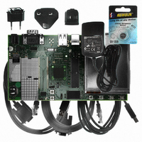
Contents
Board, Cables, Power Supply
Silicon Manufacturer
Atmel
Core Architecture
AVR
Kit Contents
Board
Svhc
No SVHC (15-Dec-2010)
Mcu Supported Families
AT91SAM9G10, ARM926EJ-S
Tool / Board Applications
Microcontroller
Rohs Compliant
Yes
For Use With/related Products
*
Lead Free Status / RoHS Status
Contains lead / RoHS non-compliant


Figure 30-8. PDC Status Register Flags Behavior
30.6.3.3
30.6.3.4
6462A–ATARM–03-Jun-09
(from master)
(from slave)
TXEMPTY
RXBUFF
TXBUFE
ENDRX
ENDTX
NPCS0
SPCK
Clock Generation
Transfer Delays
MOSI
MISO
The SPI Baud rate clock is generated by dividing the Master Clock (MCK), by a value between 1
and 255.
This allows a maximum operating baud rate at up to Master Clock and a minimum operating
baud rate of MCK divided by 255.
Programming the SCBR field at 0 is forbidden. Triggering a transfer while SCBR is at 0 can lead
to unpredictable results.
At reset, SCBR is 0 and the user has to program it at a valid value before performing the first
transfer.
The divisor can be defined independently for each chip select, as it has to be programmed in the
SCBR field of the Chip Select Registers. This allows the SPI to automatically adapt the baud
rate for each interfaced peripheral without reprogramming.
Figure 30-9
select. Three delays can be programmed to modify the transfer waveforms:
• The delay between chip selects, programmable only once for all the chip selects by writing
• The delay before SPCK, independently programmable for each chip select by writing the field
• The delay between consecutive transfers, independently programmable for each chip select
MSB
the DLYBCS field in the Mode Register. Allows insertion of a delay between release of one
chip select and before assertion of a new one.
DLYBS. Allows the start of SPCK to be delayed after the chip select has been asserted.
by writing the DLYBCT field. Allows insertion of a delay between two transfers occurring on
the same chip select
MSB
6
6
5
5
shows a chip select transfer change and consecutive transfers on the same chip
4
4
1
3
3
2
2
1
1
LSB
LSB
MSB
MSB
6
6
5
5
4
4
2
3
3
2
2
1
1
LSB
LSB
MSB
MSB
6
6
5
5
3
4
4
3
3
AT91SAM9G10
2
2
1
1
LSB
LSB
355
Related parts for AT91SAM9G10-EK
Image
Part Number
Description
Manufacturer
Datasheet
Request
R

Part Number:
Description:
MCU, MPU & DSP Development Tools KICKSTART KIT FOR AT91SAM9 PLUS
Manufacturer:
IAR Systems

Part Number:
Description:
DEV KIT FOR AVR/AVR32
Manufacturer:
Atmel
Datasheet:

Part Number:
Description:
INTERVAL AND WIPE/WASH WIPER CONTROL IC WITH DELAY
Manufacturer:
ATMEL Corporation
Datasheet:
Part Number:
Description:
Low-Voltage Voice-Switched IC for Hands-Free Operation
Manufacturer:
ATMEL Corporation
Datasheet:
Part Number:
Description:
MONOLITHIC INTEGRATED FEATUREPHONE CIRCUIT
Manufacturer:
ATMEL Corporation
Datasheet:
Part Number:
Description:
AM-FM Receiver IC U4255BM-M
Manufacturer:
ATMEL Corporation
Datasheet:
Part Number:
Description:
Monolithic Integrated Feature Phone Circuit
Manufacturer:
ATMEL Corporation
Datasheet:
Part Number:
Description:
Multistandard Video-IF and Quasi Parallel Sound Processing
Manufacturer:
ATMEL Corporation
Datasheet:
Part Number:
Description:
High-performance EE PLD
Manufacturer:
ATMEL Corporation
Datasheet:
Part Number:
Description:
8-bit Flash Microcontroller
Manufacturer:
ATMEL Corporation
Datasheet:
Part Number:
Description:
2-Wire Serial EEPROM
Manufacturer:
ATMEL Corporation
Datasheet: