AT91SAM9G10-EK Atmel, AT91SAM9G10-EK Datasheet - Page 652
AT91SAM9G10-EK
Manufacturer Part Number
AT91SAM9G10-EK
Description
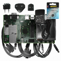
KIT DEV FOR SAM9G10 ARM
Manufacturer
Atmel
Type
MCUr
Specifications of AT91SAM9G10-EK
Contents
Board, Cables, Power Supply
Silicon Manufacturer
Atmel
Core Architecture
AVR
Kit Contents
Board
Svhc
No SVHC (15-Dec-2010)
Mcu Supported Families
AT91SAM9G10, ARM926EJ-S
Tool / Board Applications
Microcontroller
Rohs Compliant
Yes
For Use With/related Products
*
Lead Free Status / RoHS Status
Contains lead / RoHS non-compliant


38.6
38.7
652
Interrupts
Configuration Sequence
AT91SAM9G10
The LCD Controller generates six different IRQs. All the IRQs are synchronized with the internal
LCD Core Clock. The IRQs are:
Each IRQ can be individually enabled, disabled or cleared, in the LCD_IER (Interrupt Enable
Register), LCD_IDR (Interrupt Disable Register) and LCD_ICR (Interrupt Clear Register) regis-
ters. The LCD_IMR register contains the mask value for each IRQ source and the LDC_ISR
contains the status of each IRQ source. A more detailed description of these registers can be
found in
The DMA Controller starts to transfer image data when the LCDC Core is activated (Write to
LCD_PWR field of PWRCON register). Thus, the user should configure the LCDC Core and
configure and enable the DMA Controller prior to activation of the LCD Controller. In addition,
the image data to be shows should be available when the LCDC Core is activated, regardless of
the value programmed in the GUARD_TIME field of the PWRCON register.
To disable the LCD Controller, the user should disable the LCDC Core and then disable the
DMA Controller. The user should not enable LIP again until the LCDC Core is in IDLE state. This
is checked by reading the LCD_BUSY bit in the PWRCON register.
The initialization sequence that the user should follow to make the LCDC work is:
• DMA Memory error IRQ. Generated when the DMA receives an error response from an AHB
• FIFO underflow IRQ. Generated when the Serializer tries to read a word from the FIFO when
• FIFO overwrite IRQ. Generated when the DMA Controller tries to write a word in the FIFO
• DMA end of frame IRQ. Generated when the DMA controller updates the Frame Base
• End of Line IRQ. This IRQ is generated when the LINEBLANK period of each line is reached
• End of Last Line IRQ. This IRQ is generated when the LINEBLANK period of the last line of
• Create or copy the first image to show in the display buffer memory.
• If a palletized mode is used, create and store a palette in the internal LCD Palette
• Configure the LCD Controller Core without enabling it:
slave while it is doing a data transfer.
the FIFO is empty.
while the FIFO is full.
Address pointers. This IRQ can be used to implement a double-buffer technique. For more
information, see
and the DMA Controller is in inactive state.
the current frame is reached and the DMA Controller is in inactive state.
memory(See “Palette” on page 637.
– LCDCON1 register: Program the CLKVAL and BYPASS fields: these fields control the
pixel clock divisor that is used to generate the pixel clock LCDDOTCK. The value to
program depends on the LCD Core clock and on the type and size of the LCD
Module used. There is a minimum value of the LCDDOTCK clock period that
depends on the LCD Controller Configuration, this minimum value can be found in
Table 38-13 on page
pixel clock divisor can be found at the end of the section
“LCD Controller (LCDC) User Interface” on page
“Double-buffer Technique” on page
641. The equations that are used to calculate the value of the
653.
656.
“Timegen” on page 640
6462A–ATARM–03-Jun-09
Related parts for AT91SAM9G10-EK
Image
Part Number
Description
Manufacturer
Datasheet
Request
R

Part Number:
Description:
MCU, MPU & DSP Development Tools KICKSTART KIT FOR AT91SAM9 PLUS
Manufacturer:
IAR Systems

Part Number:
Description:
DEV KIT FOR AVR/AVR32
Manufacturer:
Atmel
Datasheet:

Part Number:
Description:
INTERVAL AND WIPE/WASH WIPER CONTROL IC WITH DELAY
Manufacturer:
ATMEL Corporation
Datasheet:
Part Number:
Description:
Low-Voltage Voice-Switched IC for Hands-Free Operation
Manufacturer:
ATMEL Corporation
Datasheet:
Part Number:
Description:
MONOLITHIC INTEGRATED FEATUREPHONE CIRCUIT
Manufacturer:
ATMEL Corporation
Datasheet:
Part Number:
Description:
AM-FM Receiver IC U4255BM-M
Manufacturer:
ATMEL Corporation
Datasheet:
Part Number:
Description:
Monolithic Integrated Feature Phone Circuit
Manufacturer:
ATMEL Corporation
Datasheet:
Part Number:
Description:
Multistandard Video-IF and Quasi Parallel Sound Processing
Manufacturer:
ATMEL Corporation
Datasheet:
Part Number:
Description:
High-performance EE PLD
Manufacturer:
ATMEL Corporation
Datasheet:
Part Number:
Description:
8-bit Flash Microcontroller
Manufacturer:
ATMEL Corporation
Datasheet:
Part Number:
Description:
2-Wire Serial EEPROM
Manufacturer:
ATMEL Corporation
Datasheet: