AT91SAM9G10-EK Atmel, AT91SAM9G10-EK Datasheet - Page 625
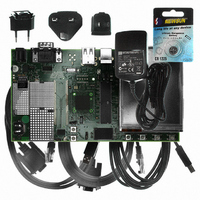
AT91SAM9G10-EK
Manufacturer Part Number
AT91SAM9G10-EK
Description
KIT DEV FOR SAM9G10 ARM
Manufacturer
Atmel
Type
MCUr
Specifications of AT91SAM9G10-EK
Contents
Board, Cables, Power Supply
Silicon Manufacturer
Atmel
Core Architecture
AVR
Kit Contents
Board
Svhc
No SVHC (15-Dec-2010)
Mcu Supported Families
AT91SAM9G10, ARM926EJ-S
Tool / Board Applications
Microcontroller
Rohs Compliant
Yes
For Use With/related Products
*
Lead Free Status / RoHS Status
Contains lead / RoHS non-compliant


Write:
0 = Can be used in the procedure to cancel transmission data. (See,
Section 37.5.2.9 “Transmit Data Cancellation” on
page
605)
1 = A new data payload has been written in the FIFO by the firmware and is ready to be sent.
This flag is used to generate a Data IN transaction (device to host). Device firmware checks that it can write a data payload
in the FIFO, checking that TXPKTRDY is cleared. Transfer to the FIFO is done by writing in the UDP_FDRx register. Once
the data payload has been transferred to the FIFO, the firmware notifies the USB device setting TXPKTRDY to one. USB
bus transactions can start. TXCOMP is set once the data payload has been received by the host.
After setting or clearing this bit, a wait time of 3 UDPCK clock cycles and 3 peripheral clock cycles is required before
accessing DPR.
• FORCESTALL: Force Stall (used by Control, Bulk and Isochronous Endpoints)
Read:
0 = Normal state.
1 = Stall state.
Write:
0 = Return to normal state.
1 = Send STALL to the host.
Refer to chapters 8.4.5 and 9.4.5 of the Universal Serial Bus Specification, Rev. 2.0 for more information on the STALL
handshake.
Control endpoints: During the data stage and status stage, this bit indicates that the microcontroller cannot complete the
request.
Bulk and interrupt endpoints: This bit notifies the host that the endpoint is halted.
The host acknowledges the STALL, device firmware is notified by the STALLSENT flag.
• RX_DATA_BK1: Receive Data Bank 1 (only used by endpoints with ping-pong attributes)
This flag generates an interrupt while it is set to one.
Write (Cleared by the firmware):
0 = Notifies USB device that data have been read in the FIFO’s Bank 1.
1 = To leave the read value unchanged.
Read (Set by the USB peripheral):
0 = No data packet has been received in the FIFO's Bank 1.
1 = A data packet has been received, it has been stored in FIFO's Bank 1.
When the device firmware has polled this bit or has been interrupted by this signal, it must transfer data from the FIFO to
microcontroller memory. The number of bytes received is available in RXBYTECNT field. Bank 1 FIFO values are read
through UDP_FDRx register. Once a transfer is done, the device firmware must release Bank 1 to the USB device by clear-
ing RX_DATA_BK1.
After setting or clearing this bit, a wait time of 3 UDPCK clock cycles and 3 peripheral clock cycles is required before
accessing DPR.
AT91SAM9G10
625
6462A–ATARM–03-Jun-09
Related parts for AT91SAM9G10-EK
Image
Part Number
Description
Manufacturer
Datasheet
Request
R

Part Number:
Description:
MCU, MPU & DSP Development Tools KICKSTART KIT FOR AT91SAM9 PLUS
Manufacturer:
IAR Systems

Part Number:
Description:
DEV KIT FOR AVR/AVR32
Manufacturer:
Atmel
Datasheet:

Part Number:
Description:
INTERVAL AND WIPE/WASH WIPER CONTROL IC WITH DELAY
Manufacturer:
ATMEL Corporation
Datasheet:
Part Number:
Description:
Low-Voltage Voice-Switched IC for Hands-Free Operation
Manufacturer:
ATMEL Corporation
Datasheet:
Part Number:
Description:
MONOLITHIC INTEGRATED FEATUREPHONE CIRCUIT
Manufacturer:
ATMEL Corporation
Datasheet:
Part Number:
Description:
AM-FM Receiver IC U4255BM-M
Manufacturer:
ATMEL Corporation
Datasheet:
Part Number:
Description:
Monolithic Integrated Feature Phone Circuit
Manufacturer:
ATMEL Corporation
Datasheet:
Part Number:
Description:
Multistandard Video-IF and Quasi Parallel Sound Processing
Manufacturer:
ATMEL Corporation
Datasheet:
Part Number:
Description:
High-performance EE PLD
Manufacturer:
ATMEL Corporation
Datasheet:
Part Number:
Description:
8-bit Flash Microcontroller
Manufacturer:
ATMEL Corporation
Datasheet:
Part Number:
Description:
2-Wire Serial EEPROM
Manufacturer:
ATMEL Corporation
Datasheet: