MA300012 Microchip Technology, MA300012 Datasheet - Page 10
MA300012
Manufacturer Part Number
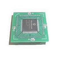
MA300012
Description
MODULE DSPIC30F SAMPLE 64QFP
Manufacturer
Microchip Technology
Specifications of MA300012
Module/board Type
dsPIC30F Plug-in Module
Lead Free Status / RoHS Status
Lead free / RoHS Compliant
For Use With/related Products
DM240001
Lead Free Status / RoHS Status
Lead free / RoHS Compliant, Lead free / RoHS Compliant


dsPIC30F
5.0
5.1
The dsPIC30F CPU module has a 16-bit (data)
modified Harvard architecture with an enhanced
instruction set, including significant support for DSP.
The CPU has a 24-bit instruction word, with a variable
length opcode field. The Program Counter (PC) is 23
bits wide and addresses up to 4M x 24 bits of user
program memory space. The actual amount of program
memory implemented, as illustrated in Figure 5-1,
varies from one device to another. A single-cycle
instruction pre-fetch mechanism is used to help
maintain
execution. All instructions execute in a single cycle,
with the exception of instructions that change the
program
instruction and the table instructions. Overhead free
program loop constructs are supported using the DO
and
interruptible at any point.
The dsPIC30F devices have sixteen 16-bit working
registers in the programmer’s model. Each of the
working registers can serve as a data, address or
address offset register. The 16th working register
(W15) operates as a software Stack Pointer for
interrupts and calls.
The dsPIC30F instruction set has two classes of
instructions: the MCU class of instructions and the DSP
class of instructions. These two instruction classes are
seamlessly integrated into the architecture and
execute from a single execution unit. The instruction
set includes many addressing modes and is designed
for optimum C compiler efficiency.
5.1.1
The data space can be addressed as 32 Kwords or 64
Kbytes and is split into two blocks, referred to as X and
Y data memory. Each memory block has its own
independent Address Generation Unit (AGU). The
MCU class of instructions operate solely through the X
memory AGU, which accesses the entire memory map
as one linear data space. Certain DSP instructions
operate through the X and Y AGUs to support dual
operand reads, which splits the data address space
into two parts. The X and Y data space boundary is
device specific.
The upper 32 Kbytes of the data space memory map
can optionally be mapped into program space at any
16K program word boundary defined by the 8-bit
Program Space Visibility Page (PSVPAG) register. The
program-to-data-space mapping feature lets any
instruction access program space as if it were data
space.
DS70043F-page 8
REPEAT
CPU ARCHITECTURE
Overview
flow,
throughput
DATA MEMORY OVERVIEW
instructions,
the
double-word
and
both
provides
move
of
which
predictable
(MOV.D)
are
FIGURE 5-1:
Arithmetic Warn. Trap Vector
Address Error Trap Vector
Reset – GOTO Instruction
Reset – Target Address
Alternate Vector Table
Stack Error Trap Vector
Interrupt Vector Table
Osc. Fail Trap Vector
Device Configuration
Program Memory
(48K instructions)
Reserved Vector
Reserved Vector
Reserved Vector
Data EEPROM
Reserved
User Flash
(Read 0’s)
(4 Kbytes)
Reserved
Registers
Reserved
Reserved
Reserved
PROGRAM SPACE
MEMORY MAP
© 2005 Microchip Technology Inc.
7FEFFE
7FF000
7FFFFE
800000
F7FFFE
F80000
F8000E
F80010
FFFFFE
000000
000002
000004
000014
00007E
000080
000084
0000FE
000100
017FFE
018000
Related parts for MA300012
Image
Part Number
Description
Manufacturer
Datasheet
Request
R

Part Number:
Description:
Manufacturer:
Microchip Technology Inc.
Datasheet:
Part Number:
Description:
Manufacturer:
Microchip Technology Inc.
Datasheet:
Part Number:
Description:
Manufacturer:
Microchip Technology Inc.
Datasheet:
Part Number:
Description:
Manufacturer:
Microchip Technology Inc.
Datasheet:
Part Number:
Description:
Manufacturer:
Microchip Technology Inc.
Datasheet:
Part Number:
Description:
Manufacturer:
Microchip Technology Inc.
Datasheet:
Part Number:
Description:
Manufacturer:
Microchip Technology Inc.
Datasheet:
Part Number:
Description:
Manufacturer:
Microchip Technology Inc.
Datasheet: