MA300012 Microchip Technology, MA300012 Datasheet - Page 65
MA300012
Manufacturer Part Number
MA300012
Description
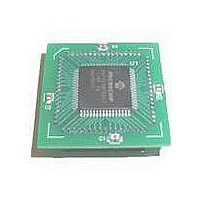
MODULE DSPIC30F SAMPLE 64QFP
Manufacturer
Microchip Technology
Specifications of MA300012
Module/board Type
dsPIC30F Plug-in Module
Lead Free Status / RoHS Status
Lead free / RoHS Compliant
For Use With/related Products
DM240001
Lead Free Status / RoHS Status
Lead free / RoHS Compliant, Lead free / RoHS Compliant


APPENDIX A:
TABLE A-1:
© 2005 Microchip Technology Inc.
AN0-AN15
AV
AV
CLKI
CLKO
CN0-CN23
COFS
CSCK
CSDI
CSDO
C1RX
C1TX
C2RX
C2TX
EMUD
EMUC
EMUD1
EMUC1
EMUD2
EMUC2
EMUD3
EMUC3
IC1-IC8
INT0
INT1
INT2
INT3
INT4
LVDIN
MCLR
OCFA
OCFB
OC1-OC8
OSC1
OSC2
Legend:
DD
SS
Pin Name
CMOS = CMOS compatible input or output Analog = Analog input
ST = Schmitt Trigger input with CMOS levels O = Output I = Input P = Power
PINOUT I/O DESCRIPTIONS
DEVICE I/O PINOUTS
AND FUNCTIONS
FOR GENERAL
PURPOSE AND
SENSOR FAMILY
Type
Pin
I/O
I/O
I/O
I/O
I/O
I/O
I/P
I/O
O
O
O
O
O
P
P
I
I
I
I
I
I
I
I
I
I
I
I
I
I
I
I
I
I
I
I
Input Buffer
ST/CMOS
ST/CMOS
Analog
Analog
Type
ST
ST
ST
ST
ST
ST
ST
ST
ST
ST
ST
ST
ST
ST
ST
ST
ST
ST
ST
ST
ST
ST
ST
—
—
—
—
—
—
P
P
Analog input channels.
AN0 and AN1 are also used for device programming data and clock
inputs, respectively.
Positive supply for Analog module.
Ground reference for Analog module.
External clock source input. Always associated with OSC1 pin
function.
Oscillator crystal output. Connects to crystal or resonator in Crystal
Input change notification inputs. Can be software programmed for
internal weak pull-ups on all inputs.
Data Converter Interface frame synchronization pin.
Data Converter Interface serial clock input/output pin.
Data Converter Interface serial data input pin.
Data Converter Interface serial data output pin.
CAN1 bus receive pin.
CAN1 bus transmit pin.
CAN2 bus receive pin.
CAN2 bus transmit pin.
Primary data I/O pin for ICD Communication Channel.
Primary clock input pin for ICD Communication Channel.
Alternate 1 data I/O pin for ICD Communication Channel.
Alternate 1 clock input pin for ICD Communication Channel.
Alternate 2 data I/O pin for ICD Communication Channel.
Alternate 2 clock input pin for ICD Communication Channel.
Alternate 3 data I/O pin for ICD Communication Channel.
Alternate 3 clock input pin for ICD Communication Channel.
Capture inputs 1 through 8.
External interrupt 0.
External interrupt 1.
External interrupt 2.
External interrupt 3.
External interrupt 4.
Low Voltage Detect input.
Master Clear (Reset) input or programming voltage input. This pin is
an active low Reset to the device.
Compare Fault A input (for Compare channels 1, 2, 3 and 4).
Compare Fault B input (for Compare channels 5, 6, 7 and 8).
Compare outputs 1 through 8.
Oscillator crystal input. ST buffer when configured in RC mode;
CMOS otherwise.
Oscillator crystal output. Connects to crystal or resonator in Crystal
Oscillator mode. Optionally functions as CLKO in RC and EC modes.
Oscillator mode. Optionally functions as CLKO in RC and EC modes.
Always associated with OSC2 pin function.
Table A-1 provides a brief description of device I/O
pinouts and functions that can be multiplexed to a port
pin. Multiple functions may exist on one port pin. When
multiplexing occurs, the peripheral module’s functional
requirements may force an override of the data
direction of the port pin.
Description
dsPIC30F
DS70043F-page 63
Related parts for MA300012
Image
Part Number
Description
Manufacturer
Datasheet
Request
R

Part Number:
Description:
Manufacturer:
Microchip Technology Inc.
Datasheet:
Part Number:
Description:
Manufacturer:
Microchip Technology Inc.
Datasheet:
Part Number:
Description:
Manufacturer:
Microchip Technology Inc.
Datasheet:
Part Number:
Description:
Manufacturer:
Microchip Technology Inc.
Datasheet:
Part Number:
Description:
Manufacturer:
Microchip Technology Inc.
Datasheet:
Part Number:
Description:
Manufacturer:
Microchip Technology Inc.
Datasheet:
Part Number:
Description:
Manufacturer:
Microchip Technology Inc.
Datasheet:
Part Number:
Description:
Manufacturer:
Microchip Technology Inc.
Datasheet: