MA300012 Microchip Technology, MA300012 Datasheet - Page 32
MA300012
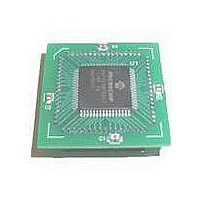
Manufacturer Part Number
MA300012
Description
MODULE DSPIC30F SAMPLE 64QFP
Manufacturer
Microchip Technology
Specifications of MA300012
Module/board Type
dsPIC30F Plug-in Module
Lead Free Status / RoHS Status
Lead free / RoHS Compliant
For Use With/related Products
DM240001
Lead Free Status / RoHS Status
Lead free / RoHS Compliant, Lead free / RoHS Compliant


dsPIC30F
9.5
The Input Capture module is useful in applications
requiring Frequency (Period) and Pulse measurement.
The dsPIC30F devices support up to eight input
capture channels.
The Input Capture module captures the 16-bit value of
the selected time base register when an event occurs
at the ICx pin. The events that cause a capture event
are listed below in three categories:
1.
2.
3.
Each input capture channel can select between one of
two 16-bit timers (Timer2 or Timer3) for the time base.
The selected timer can use either an internal or an
external clock.
Other operational features include:
• Device wake-up from capture pin during CPU
• Interrupt on input capture event
• 4-word FIFO buffer for capture values:
Input capture can also be used to provide additional
sources of external interrupts.
9.6
The Output Compare module features are quite useful
in applications that require controlled timing pulses or
PWM modulated pulse streams.
The Output Compare module has the ability to
compare the value of a selected time base with the
value of one or two compare registers (depending on
the Operation mode selected). Furthermore, it has the
ability to generate a single output pulse, or a repetitive
sequence of output pulses, on a compare match event.
Like most dsPIC30F peripherals, it also has the ability
to generate interrupts-on-compare match events.
The dsPIC30F device may have up to eight output
compare channels, designated OC1 through OC8.
Refer to the specific device data sheet for the number
of channels available in a particular device. All output
compare channels are functionally identical.
DS70043F-page 30
Sleep and Idle modes
- Interrupt optionally generated after 1, 2, 3 or
- Capture timer value on every 4th rising
- Capture timer value on every 16th rising
Simple Capture Event modes:
- Capture timer value on every falling edge of
- Capture timer value on every rising edge of
Capture timer value on every edge (rising and
falling)
Prescaler Capture Event modes:
4 buffer locations are filled
input at ICx pin
input at ICx pin
edge of input at ICx pin
edge of input at ICx pin
Input Capture Module
Output Compare/PWM Module
Each output compare channel can use one of two
selectable time bases. The time base is selected using
the OCTSEL bit (OCxCON<3>). An ‘x’ in the pin,
register or bit name denotes the specific output
compare channel. Refer to the device data sheet for the
specific timers that can be used with each output
compare channel number.
Each Output Compare module has the following modes
of operation:
• Single Compare Match mode
• Dual Compare Match mode generating:
• Simple Pulse Width Modulation mode:
9.7
The dsPIC30F Data Converter Interface (DCI) module
allows simple interfacing to devices such as audio
coder/decoders (codecs), A/D converters and D/A
converters.
The following interfaces are supported:
• Framed Synchronous Serial Transfer (Single or
• Inter-IC Sound (I
• AC-Link (AC’97) Compliant mode
Many codecs intended for use in audio applications
support sampling rates between 8 kHz and 48 kHz and
use one of the interface protocols listed above. The
DCI automatically handles the interface timing
associated with these codecs. No overhead from the
CPU is required until the requested amount of data has
been transmitted and/or received by the DCI. Up to four
data words can be transferred between CPU interrupts.
The data word length for the DCI is programmable up
to 16 bits to match the data size of the dsPIC30F CPU.
However, many codecs have data word sizes greater
than 16 bits. Long data word lengths can be supported
by the DCI. The DCI is configured to transmit/receive
the long word in multiple 16-bit time slots. This
operation is transparent to the user, and the long data
word is stored in consecutive register locations.
Figure 9-4 is a block diagram of the DCI Module. The
DCI can support up to 16 time slots in a data frame, for
a maximum frame size of 256 bits. There are control
bits for each time slot in the data frame that determine
whether the DCI will transmit/receive during the time
slot.
- Single Output Pulse
- Continuous Output Pulses
- With Fault Protection Input
- Without Fault Protection Input
Multi-Channel)
Data Converter Interface Module
2
S) Interface
© 2005 Microchip Technology Inc.
Related parts for MA300012
Image
Part Number
Description
Manufacturer
Datasheet
Request
R

Part Number:
Description:
Manufacturer:
Microchip Technology Inc.
Datasheet:
Part Number:
Description:
Manufacturer:
Microchip Technology Inc.
Datasheet:
Part Number:
Description:
Manufacturer:
Microchip Technology Inc.
Datasheet:
Part Number:
Description:
Manufacturer:
Microchip Technology Inc.
Datasheet:
Part Number:
Description:
Manufacturer:
Microchip Technology Inc.
Datasheet:
Part Number:
Description:
Manufacturer:
Microchip Technology Inc.
Datasheet:
Part Number:
Description:
Manufacturer:
Microchip Technology Inc.
Datasheet:
Part Number:
Description:
Manufacturer:
Microchip Technology Inc.
Datasheet: