MA300012 Microchip Technology, MA300012 Datasheet - Page 8
MA300012
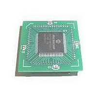
Manufacturer Part Number
MA300012
Description
MODULE DSPIC30F SAMPLE 64QFP
Manufacturer
Microchip Technology
Specifications of MA300012
Module/board Type
dsPIC30F Plug-in Module
Lead Free Status / RoHS Status
Lead free / RoHS Compliant
For Use With/related Products
DM240001
Lead Free Status / RoHS Status
Lead free / RoHS Compliant, Lead free / RoHS Compliant


dsPIC30F
3.0
Figure 3-1 shows a sample device block diagram
typical of the dsPIC30F General Purpose Product
Family. Pin functionality and pinouts for this family are
shown in Appendix A.
FIGURE 3-1:
DS70043F-page 6
AV
MCLR
V
DD
DD
, V
, AV
System Integration
Program Memory
SS
DEVICE OVERVIEW FOR
GENERAL PURPOSE AND
SENSOR FAMILIES
Data EEPROM
Address Latch
SS
(144 Kbytes)
Data Latch
(4 Kbytes)
Start-up Timer
Generation
Low Voltage
POR/BOR
Watchdog
Power-up
Oscillator
Timing
Detect
Timer
Reset
Timer
dsPIC30F5013/6013A/6014A BLOCK DIAGRAM
Control Signals
Controller
Interrupt
to Various Blocks
24
CAN1,
CAN2
Instruction
Decode &
Control
16
24
23
Control Block
PSV & Table
Data Access
24
12-bit ADC
General Purpose Family Peripherals
Timers
Central Processing Unit
16
Control
Stack
Logic
PCU
Program Counter
Y Data Bus
ROM Latch
8
PCH
Capture
Module
Input
IR
Note:
DCI
Control
Logic
Loop
16
PCL
Decode
16
Engine
DSP
The device depicted in Figure 3-1 is repre-
sentative of this family. Other devices of
the same family may vary in terms of
number of pins and multiplexing of pin
functions. Typically, smaller devices in the
family contain a subset of the peripherals
present in the device(s) shown here.
16
Compare
Module
Output
SPI1,
SPI2
Data Latch
(4 Kbytes)
Y AGU
Address
Y Data
Effective Address
Latch
RAM
16
16
16
W Reg Array
16
ALU<16>
16 x 16
16
16
16
X RAGU
X WAGU
X Data Bus
16
© 2005 Microchip Technology Inc.
Data Latch
Divide
(4 Kbytes)
UART1,
UART2
Address
Unit
X Data
I
Latch
2
RAM
C™
16
16
16
16
A B C D F G
I/O Ports
Related parts for MA300012
Image
Part Number
Description
Manufacturer
Datasheet
Request
R

Part Number:
Description:
Manufacturer:
Microchip Technology Inc.
Datasheet:
Part Number:
Description:
Manufacturer:
Microchip Technology Inc.
Datasheet:
Part Number:
Description:
Manufacturer:
Microchip Technology Inc.
Datasheet:
Part Number:
Description:
Manufacturer:
Microchip Technology Inc.
Datasheet:
Part Number:
Description:
Manufacturer:
Microchip Technology Inc.
Datasheet:
Part Number:
Description:
Manufacturer:
Microchip Technology Inc.
Datasheet:
Part Number:
Description:
Manufacturer:
Microchip Technology Inc.
Datasheet:
Part Number:
Description:
Manufacturer:
Microchip Technology Inc.
Datasheet: