CY3220LINBUS-RD Cypress Semiconductor Corp, CY3220LINBUS-RD Datasheet - Page 3
CY3220LINBUS-RD
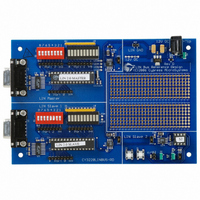
Manufacturer Part Number
CY3220LINBUS-RD
Description
KIT REF DESIGN LIN BUS
Manufacturer
Cypress Semiconductor Corp
Series
PSoC®r
Datasheet
1.CY3220LINBUS-RD.pdf
(64 pages)
Specifications of CY3220LINBUS-RD
Main Purpose
Interface, LIN
Embedded
Yes, MCU, 8-Bit
Utilized Ic / Part
CY8C27143, CY8C27443
Processor To Be Evaluated
CY8C27143-24PXI and CY8C27443-24PXI
Interface Type
RS-232
Lead Free Status / RoHS Status
Contains lead / RoHS non-compliant
Lead Free Status / RoHS Status
Lead free / RoHS Compliant, Contains lead / RoHS non-compliant
Other names
428-1926


LIN Bus 2.0 Reference Design
Contents
1.1 LIN Bus 2.0 Demonstration Kit Description .......................................................................................5
2.1 System Architecture Overview ..........................................................................................................11
3.1 Master Software Architecture ............................................................................................................15
1.2
1.3
1.4
1.5
1.6
1.7
1.8
1.9
1.10
1.11
2.2
2.3
2.4
3.2
3.3
1.1.1
Kit Contents ...............................................................................................................................5
Getting Started ...........................................................................................................................5
LIN Bus Demonstration ..............................................................................................................6
Master Node Port Pin Usage .....................................................................................................9
Slave 1 Port Pin Usage ..............................................................................................................9
Slave 2 Port Pin Usage ............................................................................................................10
Design IP .................................................................................................................................10
Demonstration Projects............................................................................................................10
Other Features .........................................................................................................................10
Support ....................................................................................................................................10
Features of the PSoC LIN Bus 2.0 Design...............................................................................11
LIN Frame ................................................................................................................................11
2.3.1
2.3.2
2.3.3
2.3.4
2.3.5
2.3.6
2.3.7
Hardware Architecture .............................................................................................................13
2.4.1
2.4.2
2.4.3
3.1.1
3.1.2
3.1.3
Device Configurations ..............................................................................................................16
3.2.1
3.2.2
3.2.3
Firmware ..................................................................................................................................17
3.3.1
3.3.2
3.3.3
3.3.4
3.3.5
Introduction ..............................................................................................................5
Break Field.............................................................................................................12
Synch Byte.............................................................................................................12
Protected Identifier.................................................................................................12
Data .......................................................................................................................12
Checksum ..............................................................................................................12
Frame Transfers on the LIN Bus............................................................................12
LIN Transceiver .....................................................................................................13
Voltage Regulator .................................................................................................13
External Pin Connections ......................................................................................13
Overview ................................................................................................................15
Foreground Processing..........................................................................................15
Timing and Interrupts .............................................................................................16
Synchro Break Configuration .................................................................................16
Data Transmission Configuration...........................................................................16
Data Reception Configuration................................................................................16
Overview ................................................................................................................17
Synchro Break Interrupt .........................................................................................17
TX Interrupt ............................................................................................................17
RX Interrupt............................................................................................................17
Bit Time Interrupt ...................................................................................................17
3.3.5.1
3.3.5.2
3.3.5.3
Basic LIN Frame ...................................................................................................11
Synchro Break Configuration ..............................................................17
Data Transmission Configuration .......................................................17
Data Reception Configuration .............................................................18
1
Related parts for CY3220LINBUS-RD
Image
Part Number
Description
Manufacturer
Datasheet
Request
R

Part Number:
Description:
KIT DEMO PSOC CAPSENSE
Manufacturer:
Cypress Semiconductor Corp
Datasheet:

Part Number:
Description:
KIT DEMO PSOC CAPSENSE SLIDE
Manufacturer:
Cypress Semiconductor Corp

Part Number:
Description:
Manufacturer:
Cypress Semiconductor Corp
Datasheet:
Part Number:
Description:
Manufacturer:
Cypress Semiconductor Corp
Datasheet:
Part Number:
Description:
Manufacturer:
Cypress Semiconductor Corp
Datasheet:
Part Number:
Description:
Manufacturer:
Cypress Semiconductor Corp
Datasheet:
Part Number:
Description:
Manufacturer:
Cypress Semiconductor Corp
Datasheet: