CY3220LINBUS-RD Cypress Semiconductor Corp, CY3220LINBUS-RD Datasheet - Page 45
CY3220LINBUS-RD
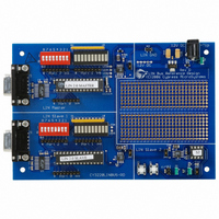
Manufacturer Part Number
CY3220LINBUS-RD
Description
KIT REF DESIGN LIN BUS
Manufacturer
Cypress Semiconductor Corp
Series
PSoC®r
Datasheet
1.CY3220LINBUS-RD.pdf
(64 pages)
Specifications of CY3220LINBUS-RD
Main Purpose
Interface, LIN
Embedded
Yes, MCU, 8-Bit
Utilized Ic / Part
CY8C27143, CY8C27443
Processor To Be Evaluated
CY8C27143-24PXI and CY8C27443-24PXI
Interface Type
RS-232
Lead Free Status / RoHS Status
Contains lead / RoHS non-compliant
Lead Free Status / RoHS Status
Lead free / RoHS Compliant, Contains lead / RoHS non-compliant
Other names
428-1926


5.1
The LIN reference design board comes with three PsoC
devices:
■
■
■
The master and slave 1 are implemented with 28-pin
CY8C27443-PXI devices and slave 2 is implemented with
an 8-pin CY8C27143-PXI device.
Note that the CD-ROM that is included with this design has
all project files for the designed-in devices as well as project
files for automotive grade devices.
Periodically, the master node sends its switch state informa-
tion to slave 1 and then polls both slaves for their switch
state information. In response, the master and slaves dis-
play the state of the information as specified by the switch-
to-display relationship. When the master sends its switch
status to slave 1, slave 1 updates its LEDs with this informa-
tion. The master updates LED 1 to LED 4 with the switch
status of SW8-SW5 of slave 1. The master updates LEDs 5
and 6 with switch status of SW1 and SW2 of slave 2. Also,
the master transmits the status of SW2 and SW1 of slave 1
to slave 2 so that slave 2 can control LEDs 1 and 2.
5.2
5.2.1
1. The LIN version is 2.0 and the baud rate is 19.2 kbps.
2. The Nodes section describes the names of the master
3. The Signals section describes the name of each signal,
4. The Dynamic Frames section describes each frame that
October 25, 2006
5.
Master
Slave 1
Slave 2
and the nodes present in the network. Master is named
as CEM. Slave 1 is named as CPM and slave 2 as DIA.
its length in bits, the publishing node and the subscribing
node(s).
is transmitted in the network, the length of the frame, the
signals that the frame carries and the offset of each sig-
nal in this frame. The frames used in the network are
VL1_CE1_Frm1 (carries the switch status of the mas-
ter), VL1_CEM_Frm2 (carries information of SW1 and
Demonstration Projects
Introduction
LIN Description File (LDF)
Description
Cypress Semiconductor – Rev. **
5. The Node Attributes section describes the slaves
6. The Schedule Table section defines the schedules that
SW2 status of slave 1 for slave 2 to control the blinking
LEDs), VL1_CPM_Frm1 (carries the resistance informa-
tion from slave 1 and the Response_Error bit),
VL1_CPM_Frm2 (carries switch status of slave 1), and
VL1_DIA_Frm1 (carries switch status of slave 2).
present in the network. Details including LIN version,
NAD, product ID, etc. are described here.
will be executed in the network. The Schedule table in
the master project will be based on this information.
43
Related parts for CY3220LINBUS-RD
Image
Part Number
Description
Manufacturer
Datasheet
Request
R

Part Number:
Description:
KIT DEMO PSOC CAPSENSE
Manufacturer:
Cypress Semiconductor Corp
Datasheet:

Part Number:
Description:
KIT DEMO PSOC CAPSENSE SLIDE
Manufacturer:
Cypress Semiconductor Corp

Part Number:
Description:
Manufacturer:
Cypress Semiconductor Corp
Datasheet:
Part Number:
Description:
Manufacturer:
Cypress Semiconductor Corp
Datasheet:
Part Number:
Description:
Manufacturer:
Cypress Semiconductor Corp
Datasheet:
Part Number:
Description:
Manufacturer:
Cypress Semiconductor Corp
Datasheet:
Part Number:
Description:
Manufacturer:
Cypress Semiconductor Corp
Datasheet: